PCB Castellated Holes (PCB Stamp Holes) Manufacturing Process: A Comprehensive Guide
Introduction to Castellated Holes
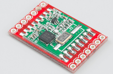
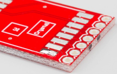
Castellated holes, commonly referred to as “PCB stamp holes” or “half holes,” are a specialized feature in printed circuit board (PCB) manufacturing that enables board-to-board connections or module attachment. These plated semi-circular cutouts along the edge of a PCB resemble the perforations between postage stamps, hence the name “stamp holes.” This 2000-word guide provides a detailed examination of the manufacturing process for PCB castellated holes, covering design considerations, fabrication steps, quality control measures, and common applications.
Design Considerations for Castellated Holes
Before delving into the manufacturing process, proper design is essential for successful castellated hole implementation:
1. Hole Size and Spacing
- Typical diameters range from 0.6mm to 1.6mm
- Maintain at least 0.2mm spacing between adjacent holes
- Keep minimum 0.5mm distance from hole edge to PCB outline
2. Pad and Annular Ring Specifications
- Minimum annular ring width of 0.15mm recommended
- Pad diameter should exceed hole diameter by at least 0.3mm
- Consider adding tear-shaped pads for improved solder flow
3. Board Edge Clearance
- Maintain 0.5mm clearance between castellated holes and internal copper features
- Avoid placing sensitive traces near board edges with stamp holes
4. Panelization Design
- Include adequate spacing between boards in the panel (typically 2-3mm)
- Design breakaway tabs or mouse bites for easy depanelization
- Consider routing paths for clean separation after plating

Step-by-Step Manufacturing Process
Step 1: PCB Panel Preparation
The process begins with standard PCB fabrication up to the drilling stage:
- Laminate copper-clad substrate material (typically FR-4)
- Apply dry film resist and pattern using photolithography
- Etch copper to create desired circuit patterns
- Strip remaining resist and clean panels
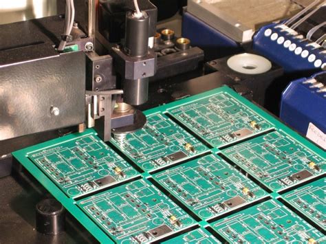
Step 2: Drilling Castellated Holes
- Load PCB panel into CNC drilling machine
- Use specialized drill bits (typically tungsten carbide)
- Standard drill sizes: 0.6mm, 0.8mm, 1.0mm, 1.2mm, 1.6mm
- Drill speed: 60,000-100,000 RPM depending on bit size
- Drill complete through-holes along planned board edges
- Holes are drilled fully through the panel at this stage
- Maintain precise positioning relative to board outline
- Perform visual inspection of drilled holes for debris or irregularities
Step 3: Electroless Copper Deposition
- Clean drilled panels to remove drilling debris
- Apply chemical micro-etch to roughen surfaces
- Catalyze panel surfaces with palladium-based activator
- Deposit thin (0.5-1μm) copper layer through electroless plating
- Provides conductive base for subsequent electroplating
- Ensures uniform coverage in holes and on surfaces
Step 4: Dry Film Lamination and Patterning
- Laminate photosensitive dry film resist over panel surfaces
- Expose with UV light through artwork film
- Pattern protects areas to remain as copper features
- Develop to remove unexposed resist, creating plating mask
- Inspect for complete resist coverage over non-plated areas
Step 5: Electroplating Process
- Copper electroplating:
- Builds up copper thickness to 20-25μm
- Ensures reliable conductivity in castellated holes
- Typical plating time: 60-90 minutes
- Optional tin or gold plating:
- Tin plating (2-5μm) for solderability
- Gold plating (0.05-0.1μm) for oxidation resistance
- Strip plating resist after electroplating completion
Step 6: Final Copper Etching
- Apply second layer of etch resist over plated patterns
- Etch away exposed copper to isolate circuits
- Ammoniacal or acidic copper etchants typically used
- Etch time carefully controlled to prevent undercutting
- Strip remaining resist, revealing final copper features
Step 7: Solder Mask Application
- Clean panels and apply liquid photoimageable solder mask
- Expose through artwork to pattern mask openings
- Leave castellated holes and contact pads exposed
- Develop to remove unexposed mask material
- Cure through UV and thermal processes
Step 8: Surface Finish Application
- Apply final surface finish to exposed copper:
- HASL (Hot Air Solder Leveling): Most common
- ENIG (Electroless Nickel Immersion Gold): For fine-pitch
- Immersion Silver or Tin: Alternative finishes
- Ensure complete coverage of castellated hole surfaces
Step 9: Routing Castellated Holes
This critical step creates the characteristic half-hole profile:
- Mount panel in precision routing machine
- Use specialized carbide routing bits (0.8-2.0mm diameter)
- Route along board edges intersecting drilled holes:
- Path must precisely bisect each hole
- Typical routing speed: 20,000-30,000 RPM
- Feed rate: 0.5-1.5 meters/minute
- Collect routing dust with vacuum system
- Inspect routed edges for clean half-hole formation
Step 10: Quality Control and Testing
- Visual inspection:
- Verify complete plating in castellated holes
- Check for burrs or rough edges
- Confirm proper hole bisection
- Dimensional verification:
- Measure hole diameters and positions
- Verify board outline accuracy
- Electrical testing:
- Conduct continuity tests through plated holes
- Check for shorts between adjacent holes
- Solderability testing (sample boards):
- Verify proper wetting of castellated holes
- Assess solder joint formation quality
Step 11: Depanelization (If Applicable)
- For panelized designs, separate individual boards:
- Use routing, scoring, or breakaway tab methods
- Clean board edges to remove any residual material
- Perform final visual inspection of castellated holes
Advanced Manufacturing Techniques
Laser-Drilled Castellated Holes
- Used for ultra-small holes (<0.3mm diameter)
- CO2 or UV lasers create precise micro-vias
- Allows higher density edge connections
Sequential Lamination Method
- Create sub-composites with pre-cut edges
- Laminate together with prepreg layers
- Allows castellated holes on inner layers
Plugged Castellated Holes
- Fill holes with conductive or non-conductive material
- Re-drill after plating for improved reliability
- Useful for high-vibration applications
Common Challenges and Solutions
1. Incomplete Hole Plating
- Solution: Optimize electroless copper process parameters
- Increase agitation during electroplating
2. Rough Hole Edges
- Solution: Use sharper routing bits
- Adjust routing speed and feed rates
- Implement post-route deburring process
3. Solder Mask Bleeding
- Solution: Modify solder mask viscosity
- Adjust pre-cure conditions before exposure
4. Copper Peeling at Edges
- Solution: Improve copper adhesion through surface treatment
- Reduce mechanical stress during routing
Applications of Castellated Holes
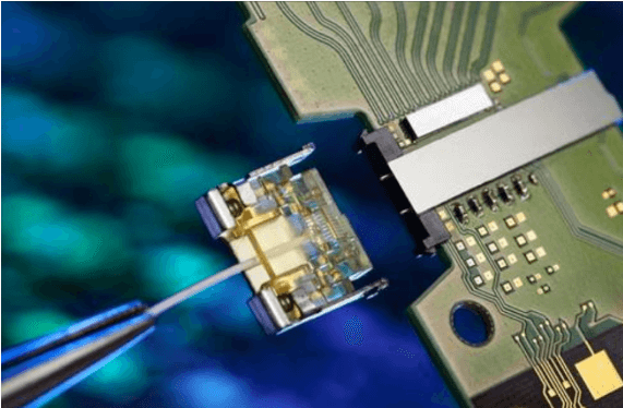
1. Board-to-Board Connections
- Stacked PCB configurations
- Daughterboard attachment
2. Modular Circuit Components
- RF modules
- Wireless communication boards
- Sensor arrays
3. Edge-Soldered Devices
- System-on-module designs
- Embedded computing units
4. Consumer Electronics
- Wearable devices
- Compact IoT products
Conclusion
The manufacturing of PCB castellated holes requires precise execution of multiple fabrication steps, from initial drilling through final routing. By understanding the complete process flow—including design preparation, plating operations, routing techniques, and quality control measures—manufacturers can produce reliable castellated holes that meet the growing demand for compact, modular electronic assemblies. Proper implementation of these stamp hole techniques enables innovative PCB architectures while maintaining robust mechanical and electrical connections.
As electronic devices continue to shrink in size while increasing in complexity, castellated hole technology will play an increasingly important role in PCB design and manufacturing. Mastery of these processes allows for the creation of more compact, reliable, and cost-effective electronic systems across numerous industries.