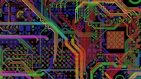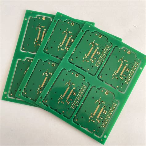
PCB circuit board layer full resolution
PCB design If you need to connect multiple boards to a larger system and provide interconnections between them, you may use a backplane to arrange and cascade these boards.
The backplane is an advanced board, which borrows some elements from high-speed design, mechanical design, high-voltage/high-current design and even RF design. These boards are commonly used in mission-critical defense systems, telecommunications systems, and data centers. They use their own set of standards, which exceed the reliability requirements of IPC.
Although backplanes follow specific standards that many other PCBs do not have, many PCB designers are familiar with the concepts involved in layout and routing.
At first, the large number of connectors and networks and the narrow space on a typical backplane seemed difficult. Nevertheless, some simple strategies can still help you maintain the organizational structure and complete the backplane design while ensuring high reliability. My hope is that you will learn some strategies for implementing the next backplane design in terms of wiring and layout to balance reliability and signal integrity. Without more content, let us jump into this rich field of PCB design.
Getting started with backplane design
Backplane design, layout and wiring entry need to take many angles. These designs can be difficult because you may find yourself managing thousands of connections on large boards with limited space and number of layers. In addition, the backplane may actually be involved in powering the daughter cards, and each daughter card may be pulling multiple amperes of current through various high-speed devices. This means that your backplane may need to support about 100 A of current.
Since the main function of the backplane is to provide connections between multiple boards in a large system,
everything revolves around the connectors you will use, and these connectors are the starting point for your design. The following are some of the basic tasks involved in backplane design:
Pinout: The first step is to determine the pinout on the connector to support the required routing topology. I will describe this further below.
Mechanical requirements: In addition to the correct placement of the daughter board connector, guide pins are also used to ensure correct fit and structural integrity. The image at the bottom of the list shows typical guide pins used with backplane connectors.
Material selection: For high-speed backplanes, this is a key point in the design process. Since the backplane can be very large, any signal that needs to propagate over the entire plane can suffer significant losses. Low-loss laminates with tight glass weave are needed to minimize insertion loss on long interconnects.
Power and grounding strategies: For backplanes that need to provide high power to a large number of daughter boards, you will need a power and grounding strategy that helps maintain low temperatures. The ground/power plane layout on different plane layers should also provide isolation for high-speed signals isolated on the circuit board.
Number of layers: The number of layers required for the backplane will depend on the number of plane layers and the number of signal layers required. The backplane can have up to 24 layers with a thickness of several millimeters, which can meet all design requirements.
The points above are the same as those to be considered in any other high-speed design. However, once you work on the backplane, the situation is different because the pinout of the connector restricts the wiring. This is an important part of the backplane design and should be planned carefully.

All involving connectors, pin assignments and wiring
Most of the focus of the initial design phase will be on the connectors on the backplane. Choosing connectors (including connectors for backplanes) is both an art and a science, and these connectors will become the main determinants of signal integrity. To ensure that the signal is not excessively attenuated at the connector tracking interface, simulation is very important.
The pin arrangement in the connector is also very important because it helps simplify the wiring of each layer.
In particular, your pinout should achieve two goals:
It should be designed to prevent signals on a given layer from crossing each other when routing signals to all connectors on the backplane bus. If done correctly, you may be able to eliminate some signal layers.
Ideally, when reaching the pins on each connector, the wiring should be smooth across the entire backplane (mostly horizontal).
It is best done in a row-by-row manner, similar to the differential pair routing shown below.
Note how the pins on each connector are staggered in each column, allowing the traces in the differential pair to enter between the rows of connector pins. If all the pins are in the same column, then I need 2 layers instead of 1 to make the wiring shown below.
Considering all these design requirements, I found it difficult to achieve all these balances in my first backplane, and we didn’t even make the initial component placement.
You won’t have much freedom in component placement, but as long as the pins are arranged and consistent throughout the connector, you can keep things organized when routing signals through the backplane. Some other tips to help you succeed include:
Minimize the transition of high-speed signals.
Each via will increase the insertion loss of the interconnect, and it is necessary to minimize the insertion loss.
High-speed back drilling through transition. Reverse drilling will increase the cost, but will minimize the stub discontinuity on the long transmission line.
Don’t be afraid to fall to the ground. Using ground backflow helps to isolate between different high-speed trace groups, ensures a consistent impedance curve, and provides sufficient conductors for high return currents.
Make all unused signal layers become plane layers. If you are going to supply power through the backplane, don’t worry about throwing additional power boards into the stack. Distributing current among multiple power layers helps keep the PDN cool.
Backplane design is not suitable for the faint-hearted because it requires multiple professions to succeed. However, if you have the right team of designers and a complete set of design tools, you can complete most aspects of the design process on one platform. You will be able to complete the backplane design and prepare for production through a program.