PCB Component Pad Design: Essential Techniques and Best Practices
Introduction
Printed Circuit Board (PCB) design is a complex process that requires careful attention to numerous details, with component pad design being one of the most critical aspects. Proper pad design ensures reliable solder joints, facilitates manufacturing, and improves the overall quality and longevity of the electronic assembly. This article explores the essential techniques and best practices for designing effective PCB component pads.
1. Understanding Pad Fundamentals
1.1 Pad Types and Their Applications
PCB pads come in various forms, each serving specific purposes:
- Through-hole pads: Used for components with leads that pass through the board
- Surface mount (SMD) pads: For components mounted directly on the board surface
- Thermal pads: Designed to manage heat dissipation for power components
- Test pads: Used for testing and debugging purposes
1.2 Pad Geometry Considerations
The shape and size of pads significantly impact solderability and mechanical strength:
- Rectangular pads: Common for surface mount devices (SMDs)
- Circular pads: Typically used for through-hole components
- Oval pads: Offer a compromise between circular and rectangular
- Custom shapes: For specialized components or high-density designs
2. Key Design Parameters for Effective Pads
2.1 Size and Dimensional Accuracy
Proper pad sizing is crucial for reliable solder joints:
- Land pattern dimensions: Should match component specifications
- Tolerance considerations: Account for manufacturing variations
- IPC standards: Follow IPC-7351 for standardized land patterns
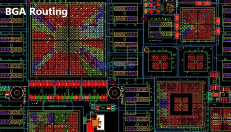
2.2 Pad-to-Pad Spacing
Adequate spacing prevents solder bridging and manufacturing defects:
- Minimum clearance: Typically 0.2mm for most applications
- High-density designs: May require tighter spacing with special considerations
- Voltage considerations: Increase spacing for high-voltage applications
2.3 Pad Orientation and Alignment
Proper orientation affects solder flow and joint formation:
- Component alignment: Pads should mirror component lead configuration
- Wave soldering considerations: Pad orientation affects solder flow
- Repair and rework: Design for accessibility during maintenance
3. Specialized Pad Design Techniques
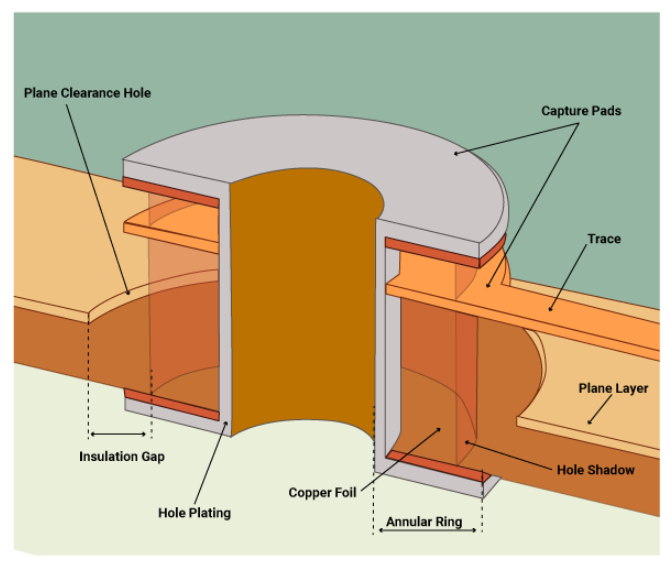
3.1 Thermal Relief Pads
Essential for components requiring heat dissipation or thermal management:
- Thermal connections: Use spoke patterns to balance heat transfer
- Ground planes: Implement thermal relief for through-hole connections
- Power components: Ensure adequate thermal mass for heat dissipation
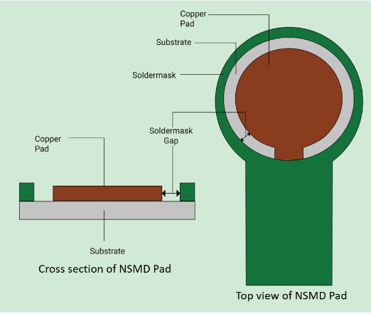
3.2 Solder Mask and Paste Considerations
Proper solder mask and paste application improves manufacturability:
- Solder mask defined (SMD) vs non-solder mask defined (NSMD) pads
- Solder paste stencil design: Affects volume and distribution
- Tented vias: Protection against solder wicking
3.3 High-Frequency and RF Pad Design
Special considerations for high-speed and RF applications:
- Controlled impedance: Pad design affects signal integrity
- Parasitic effects: Minimize parasitic capacitance and inductance
- Grounding techniques: Proper RF grounding through pads
4. Manufacturing Considerations in Pad Design
4.1 Design for Manufacturing (DFM)
Ensure designs are optimized for production processes:
- Soldering process compatibility: Wave, reflow, or hand soldering
- Assembly tolerances: Account for placement accuracy
- Inspection requirements: Design for automated optical inspection (AOI)
4.2 Handling Component Variations
Accommodate variations in component sizes and packages:
- Tolerance stacking: Consider cumulative tolerances
- Alternative components: Design for substitute parts
- Package variations: Account for different manufacturer specifications
4.3 Testability and Rework
Design pads to facilitate testing and repair:
- Test point incorporation: Ensure accessibility
- Rework considerations: Allow space for repair tools
- Debug access: Provide probing points when needed
5. Advanced Pad Design Techniques
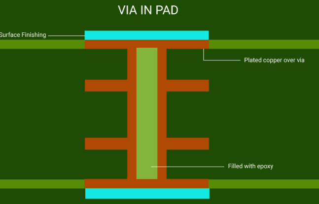
5.1 HDI and Microvia Technology
Techniques for high-density interconnect designs:
- Microvia-in-pad: For space-constrained designs
- Via filling and capping: Planarization for fine-pitch components
- Stacked and staggered vias: Managing high-density interconnects
5.2 Flexible and Rigid-Flex PCB Pads
Special considerations for flexible circuits:
- Pad reinforcement: Additional support for flex areas
- Strain relief: Preventing pad lifting during flexing
- Adhesive selection: Compatible with flexible materials
5.3 3D Component Integration
Designing for emerging packaging technologies:
- Embedded components: Pad design for buried elements
- Package-on-package (PoP): Pad arrangements for stacked ICs
- System-in-package (SiP): Integration challenges
6. Common Pitfalls and How to Avoid Them
6.1 Typical Design Mistakes
Frequent errors in pad design:
- Inadequate pad size: Leading to weak solder joints
- Improper thermal relief: Causing soldering or heat dissipation issues
- Incorrect spacing: Resulting in bridging or open circuits
6.2 Verification and Validation
Methods to ensure proper pad design:
- Design rule checks (DRC): Automated verification
- 3D modeling: Visualizing component placement
- Prototyping: Physical verification before full production
Conclusion
Effective PCB component pad design requires a balance of electrical, mechanical, and manufacturing considerations. By understanding the fundamental principles, applying specialized techniques where needed, and considering the manufacturing process, designers can create reliable, manufacturable PCB layouts. Continuous learning and adaptation to new component technologies and packaging methods remain essential for maintaining excellence in PCB pad design.
As the electronics industry continues to evolve with smaller components and more complex packaging, pad design will remain a critical skill for PCB designers. Mastering these techniques ensures robust, reliable electronic products that can be efficiently manufactured at scale.