
PCB Copper Balance: Preventing Bow and Twist in Manufacturing
Warped PCBs lead to assembly failures, component misalignment, and rejected production runs. A 2025 industry survey found that copper imbalance accounts for 35% of all PCB warpage defects, costing manufacturers thousands in rework and scrap. Understanding copper balance isn’t just about meeting specifications—it’s about ensuring your boards stay flat through manufacturing and reliable through their service life.
This guide explains how copper distribution affects board flatness, how to calculate copper percentage across layers, and proven design strategies to prevent bow and twist before fabrication begins. Learn more about our PCB manufacturing capabilities and rigid flex PCB solutions.
What is PCB Copper Balance?
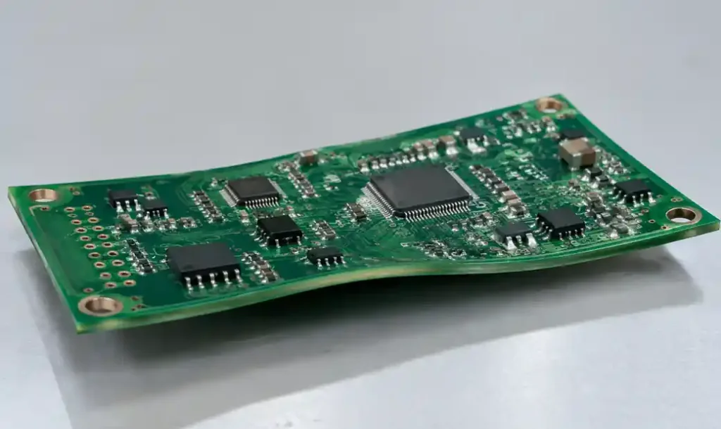
PCB copper balance refers to the even distribution of copper features across all layers of a circuit board. Balanced copper means each layer has similar copper coverage percentages, and the stackup is symmetrical from top to bottom. When copper is distributed unevenly—dense traces on one layer opposite sparse routing on another—the board experiences mechanical stress during thermal cycling that manifests as warpage.
Copper and FR-4 substrate have different coefficients of thermal expansion (CTE). Copper expands at approximately 17 ppm/°C, while FR-4 expands at 15-20 ppm/°C in the z-axis. During lamination at 180-200°C, these materials heat and expand together. Upon cooling, unbalanced copper distribution locks in internal stresses that cause the board to bow or twist.
Understanding Bow and Twist in PCBs
Bow describes a cylindrical deformation where the board curves while all four corners remain approximately coplanar. Twist occurs when one corner lifts while the other three lie flat on a reference surface, creating a diagonal warpage pattern.
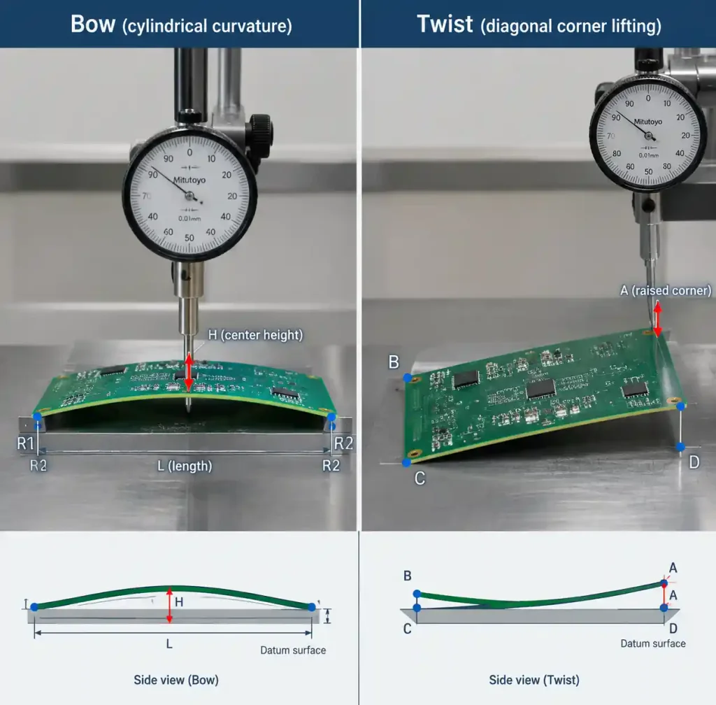
According to IPC-TM-650 section 2.4.22, bow and twist are measured as a percentage of the board’s diagonal length. Industry acceptance criteria per IPC-6012 are:
| Board Type | Maximum Bow/Twist |
|---|---|
| Surface mount assemblies | ≤0.75% |
| Non-SMT boards | ≤1.5% |
For a 150mm × 100mm board (diagonal = 180mm), the maximum allowable deviation for SMT assemblies is 1.35mm. Exceeding this tolerance causes placement errors during automated assembly, solder joint failures, and component standoff issues.
Root Causes of Copper Imbalance
Asymmetric Layer Stackups
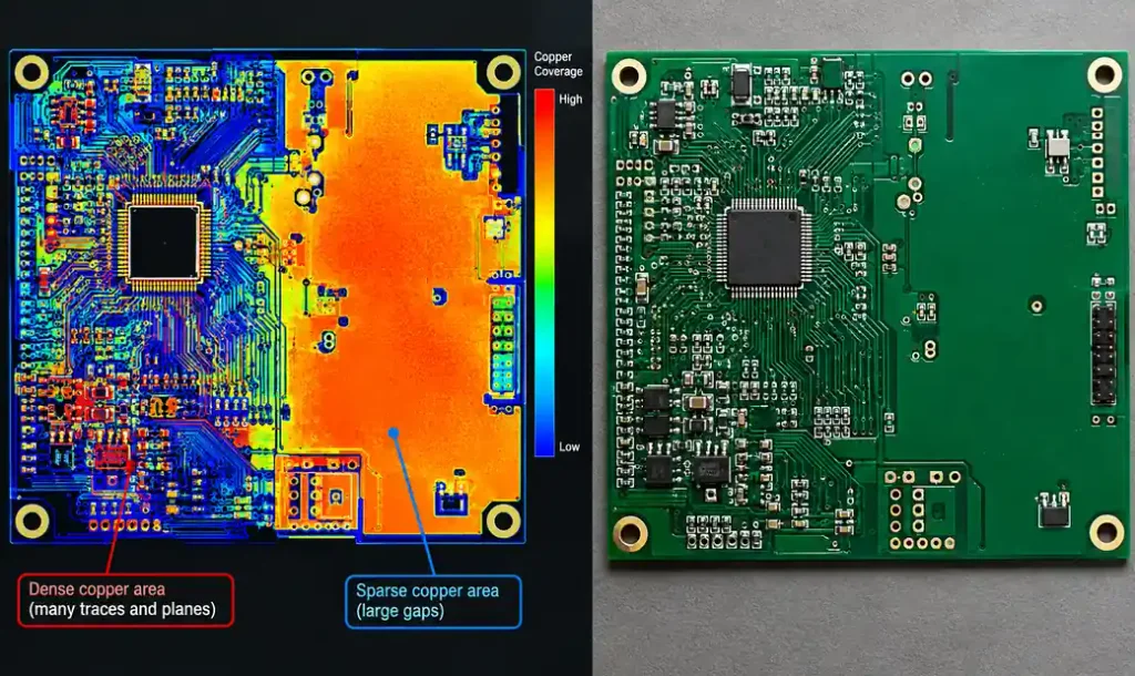
When signal layers with 30% copper coverage sit opposite power planes with 90% coverage, the stackup lacks symmetry. During lamination, the heavy copper side contracts more than the light copper side, bending the board permanently.
Uneven Copper Distribution Within Layers
Large open areas on one side of a layer paired with dense routing on the opposite side create localized stress points. These imbalances amplify during reflow soldering when boards reach 260°C peak temperatures.
Heavy Copper Applications
Boards with 3oz or 4oz copper require extra attention. Heavy copper increases thermal mass and exaggerates CTE mismatch effects. Longer etch times for thick copper can also lead to uneven material removal if distribution isn’t controlled.
How to Calculate Copper Percentage
Copper percentage represents the proportion of a layer’s area occupied by copper features—traces, pours, pads, and planes.
Manual Estimation Method:
- Export each layer as a Gerber file
- Import into CAD software that calculates area
- Divide copper area by total board area
- Express as percentage
Automated CAM Tools:
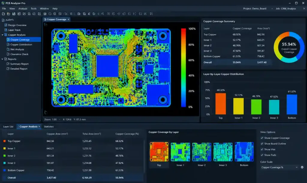
Modern fabrication CAM software calculates copper percentage automatically. Designers should target these ranges:
| Layer Type | Target Copper Coverage |
|---|---|
| Signal layers | 30-50% |
| Power/ground planes | 70-90% |
| Balanced stackup tolerance | ±15% between paired layers |
For a 6-layer stackup, aim for symmetry: if Layer 1 (top) has 40% copper, Layer 6 (bottom) should have 35-45%. Similarly, internal layer pairs (L2/L5 and L3/L4) should mirror each other.
Design Strategies for Copper Balance
Symmetrical Stackup Design
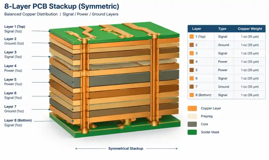
Design stackups that mirror from the centerline. For an 8-layer board:
- L1 (signal) ↔ L8 (signal)
- L2 (ground) ↔ L7 (ground)
- L3 (signal) ↔ L6 (signal)
- L4 (power) ↔ L5 (power)
Match copper weights between paired layers. If L2 uses 1oz copper, L7 should also use 1oz. Avoid mixing 0.5oz and 2oz copper in mirrored positions.
Copper Thieving and Dummy Fills
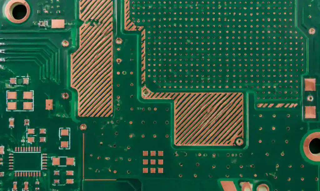
Copper thieving adds non-functional copper patterns to sparse areas, balancing distribution without affecting circuit function. Common patterns include:
- Dot grids: 0.2-0.5mm dots spaced 1-2mm apart
- Hatched fills: 45° diagonal lines with 0.5mm spacing
- Isolated pads: Small squares in open areas
Best practices for copper thieving:
- Keep thieving features at least 0.5mm from functional traces
- Use grid patterns for high-frequency designs to minimize coupling
- Connect thieving to ground through stitching vias where possible
- Coordinate with your PCB manufacturer—many add thieving during CAM processing
Copper Pour Strategies
When flooding layers with copper:
- Use hatched pours for signal layers to reduce capacitive coupling
- Keep solid pours for power and ground planes
- Maintain clearances: 0.2-0.3mm around traces, 0.5mm around vias
- Add thermal reliefs at via and pad connections to aid soldering
Avoid large solid copper areas on signal layers opposite sparse routing. Instead, use 50% hatched fills that provide grounding while balancing copper distribution.
Manufacturability Limits and DFM Guidelines
PCB manufacturers specify copper balance tolerances in their capability tables. Typical production limits:
Standard capability:
- Layer-to-layer copper variance: ±20%
- Total stackup symmetry: within 15% top-to-bottom
Advanced capability:
- Layer-to-layer variance: ±10%
- Critical for >20 layer boards and HDI constructions
When designing outside these ranges, manufacturers may add balancing features during panel preparation or require design revisions.
Verification Before Fabrication
Before sending Gerbers to production:
- Review copper distribution reports from your CAM tool
- Check stackup symmetry using DFM software
- Request pre-production DFM review from your manufacturer
- Specify bow/twist requirements in fabrication notes (typically IPC-6012 Class 2 or Class 3)
For high-reliability applications—automotive, medical, aerospace—request tighter tolerances (≤0.5%) and post-fabrication flatness inspection reports.
Material Selection and Process Control
Substrate Material Considerations
High-Tg FR-4 (Tg ≥170°C) offers better dimensional stability than standard FR-4 (Tg 130-140°C). For demanding applications, consider:
- Polyimide: Lower CTE, better for flex and rigid-flex designs
- Rogers laminates: Consistent Dk and low moisture absorption for high-frequency applications
- Ceramic substrates: Near-zero CTE for extreme environments
Manufacturing Process Parameters
Fabricators control bow and twist through:
- Press cycle optimization: Balanced heat and pressure during lamination
- Panel tooling: Symmetric placement on production panels
- Cooling rate control: Gradual temperature reduction to minimize locked-in stress
- Post-cure baking: Stress relief at controlled temperatures
Work with manufacturers who document their process controls for critical boards.
FAQ
What is the acceptable copper imbalance for a 4-layer board?
For standard 4-layer boards, aim for ±15% copper coverage between top and bottom layers, and between the two internal layers. IPC-6012 Class 2 tolerates up to 0.75% bow/twist, which typically requires keeping layer pairs within 20% copper variance.
Can copper balance be fixed after fabrication?
No. Once lamination completes and stresses lock in, warpage cannot be corrected without re-fabricating the board. Some manufacturers attempt flattening through controlled heating, but this risks delamination and rarely meets assembly tolerances.
How does copper balance affect HDI PCBs?
HDI boards with microvias and sequential lamination are more sensitive to copper imbalance. Each lamination cycle introduces thermal stress. Maintaining symmetry in build-up layers is critical—mirror your microvia patterns and copper pours between top and bottom build-ups.
What tools calculate copper distribution automatically?
Modern EDA tools like Altium Designer, Cadence Allegro, and KiCad include copper balancing analysis. CAM software such as Genesis and CAM350 provides layer-by-layer distribution reports during Gerber output.
When should I use copper thieving vs. solid copper pours?
Use copper thieving when you need minor adjustments (5-10% coverage) without affecting circuit behavior. Use solid copper pours for larger coverage needs on power/ground layers. For signal layers with high-speed traces, prefer hatched or grid-pattern thieving to avoid introducing unintended capacitance.
Conclusion
Copper balance directly determines whether your PCB survives manufacturing without warpage defects. Symmetric stackup design, calculated copper distribution targeting ±15% between layer pairs, and strategic use of copper thieving prevent bow and twist before lamination begins. Modern CAM tools make copper analysis straightforward—use them early in your design cycle, not after layout completion.
Verify copper distribution during design reviews, specify IPC-6012 flatness requirements in your fabrication documentation, and partner with manufacturers who document their process controls. For high-layer-count boards, HDI constructions, or heavy copper applications, request pre-production DFM analysis to identify imbalance issues before tooling.
Andwin Circuits specializes in manufacturing complex PCBs with strict copper balance control. Our process includes automated copper distribution analysis, symmetrical stackup verification, and post-fabrication flatness inspection for boards up to 50 layers. Contact our engineering team for a free DFM review of your next project.
Sources
- Understanding and Preventing PCB Warpage with Copper Balancing
- Balanced Copper Distribution and Weight in PCBs
- PCB Bow and Twist: Causes, Prevention & Measurement
- PCB Warpage Control: Mitigating Bow and Twist
- PCB Copper Balancing: Warp Control & Yield Boost
- IPC-TM-650 Test Methods Manual
- Copper Thieving in PCBs
- How to Balance Copper in a Multilayer PCB