
PCB Silkscreen: Design Rules and Readability Optimization
Assembly technicians lose an average of 15-30 seconds per component when silkscreen markings are unclear or missing. On a 200-component board, poor silkscreen design adds 50-100 minutes to assembly time and increases polarity errors by 40%. Industry data shows that 18% of PCB assembly rework stems from misidentified components due to inadequate silkscreen markings.
When designing PCBs for manufacturing, the silkscreen layer determines whether your boards assemble correctly the first time or require costly rework. This guide provides specific dimensional rules, color selection criteria, and placement strategies based on IPC standards and production floor feedback from high-volume PCB manufacturers.
What Is PCB Silkscreen and Why It Matters
PCB silkscreen is the layer of epoxy ink printed onto the board surface carrying reference designators, component outlines, polarity marks, and assembly instructions. Unlike copper traces or solder mask, silkscreen performs no electrical function—its purpose is purely informational.
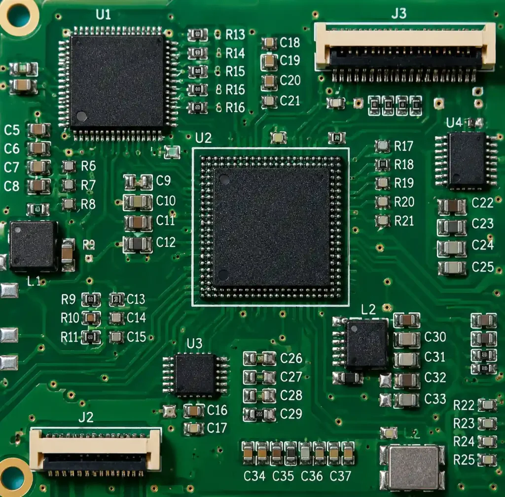
Silkscreen quality directly impacts assembly speed, inspection accuracy, and field service. Boards with clear 1.2mm-tall reference designators assemble 35% faster than those with 0.8mm text. Polarity marks placed 0.3mm from component edges reduce installation errors from 12% to under 2%, critical for PCB assembly services.
Modern high-density designs with HDI PCB packages, 0201 passives, and dense connectors make silkscreen placement challenging. You must balance readability with space constraints while ensuring no silkscreen overlaps pads.
Minimum Text Size and Line Width Standards
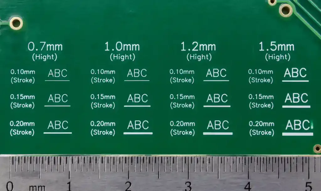
IPC-SM-782 establishes baseline silkscreen dimensions. Standard screen printing requires minimum stroke width of 0.15mm (6 mils) and character height of 1.0mm (40 mils) for reliable reproduction. Text smaller than these minimums may blur or disappear during printing.
For reference designators and critical markings, specify 1.2-1.5mm character height with 0.15-0.20mm stroke width. When space allows, use 1.5mm height—operators can read these markings from 30cm away.
| Text Application | Minimum Height | Recommended Height | Stroke Width | Readability Distance |
|---|---|---|---|---|
| Reference designators | 1.0mm (40 mils) | 1.2-1.5mm (47-59 mils) | 0.15-0.20mm (6-8 mils) | 15-30cm |
| Component values | 0.8mm (32 mils) | 1.0mm (40 mils) | 0.12-0.15mm (5-6 mils) | 10-20cm |
| Warning text | 1.5mm (59 mils) | 2.0mm (79 mils) | 0.20-0.25mm (8-10 mils) | 30-50cm |
| Fine-pitch markings | 0.7mm (28 mils) | 0.8mm (32 mils) | 0.10mm (4 mils) | Requires magnification |
LPI (liquid photo-imageable) silkscreen enables finer resolution down to 0.10mm stroke width and 0.7mm character height, suitable for dense layouts. However, LPI costs 15-30% more.
Maintain a 6:1 to 8:1 aspect ratio between character height and stroke width. A 1.2mm tall character should use 0.15-0.20mm stroke width.
Silkscreen Color Selection and Contrast
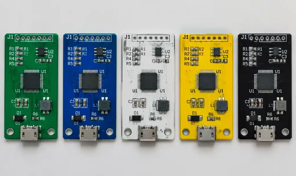
White silkscreen on green solder mask remains the industry standard, providing 85% optical contrast—the highest of common combinations.
Black silkscreen works best on white, yellow, or red solder mask, delivering 75-80% contrast. Never specify black on green or dark blue solder mask—contrast drops below 40%. Yellow silkscreen on blue solder mask provides 70% contrast for brand-specific colors.
For boards requiring UV resistance, specify epoxy-based white silkscreen rather than standard ink. Standard silkscreen yellows under prolonged UV exposure, reducing contrast by 15-20% over 2-3 years.
| Color Combination | Contrast | Best Use | Avoid When |
|---|---|---|---|
| White on green | 85% | Standard boards, high-volume | Never—always works |
| White on blue | 80% | Consumer electronics | Aesthetic concerns only |
| Black on white | 80% | Medical devices, clean room | Requires white soldermask |
| Black on yellow | 75% | Industrial equipment | Cost-sensitive projects |
| Yellow on blue | 70% | Brand-specific designs | High-precision assembly |
Never print silkscreen in copper—copper oxidizes and provides no contrast against solder mask. Always use proper epoxy ink formulated for PCB applications.
Reference Designator Placement Rules
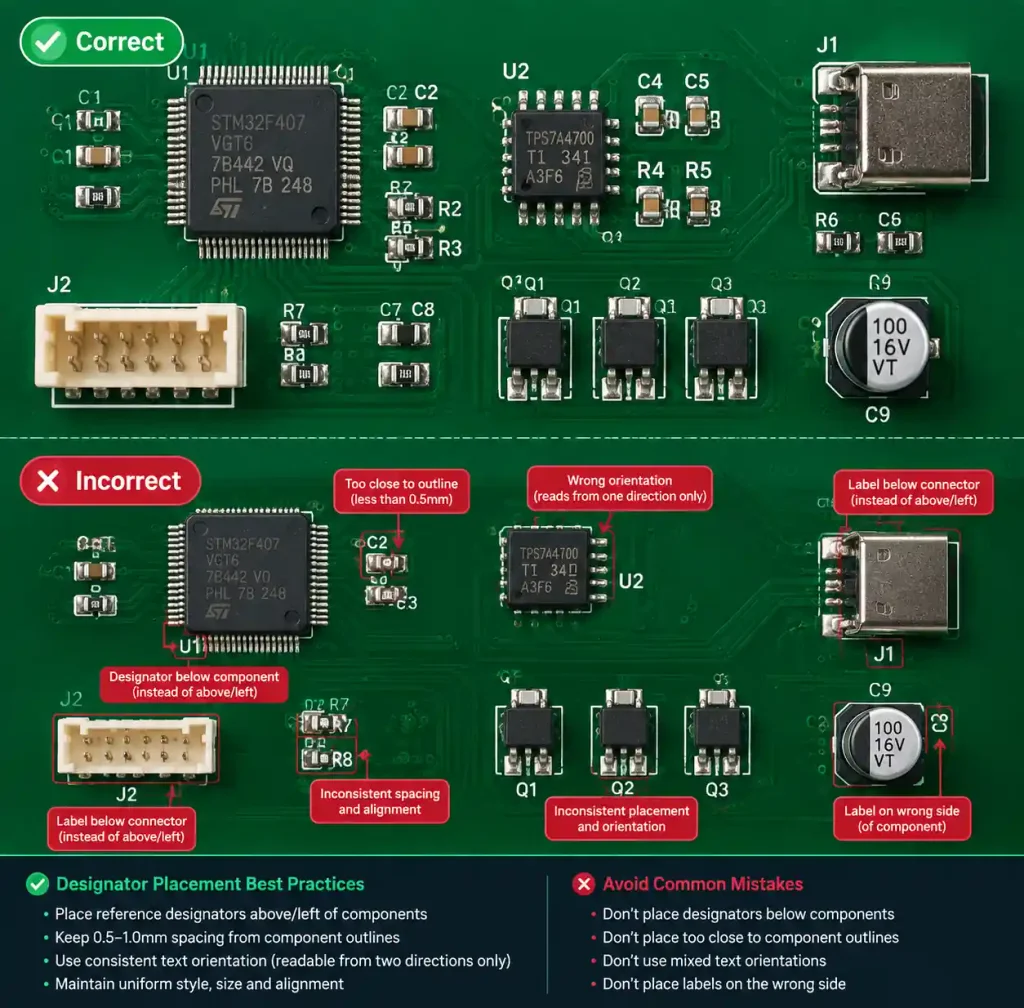
Reference designators identify components using standardized prefixes: R for resistors, C for capacitors, U for ICs, J for connectors. Place designators consistently—either above or left of the component outline.
Position designators 0.5-1.0mm away from component outlines to prevent overlap with parts. For IC packages, place designators outside pin 1 indicators where they won’t be covered by the component body.
Orient all designators to read from two directions maximum—bottom-to-top and left-to-right. Boards requiring rotation more than twice during assembly slow down placement and increase error rates.
Never hide designators under components—a reference you can’t see after assembly provides no value during rework or field service. For bottom-side components, print designators on the bottom silkscreen layer.
Component Polarity and Orientation Marking
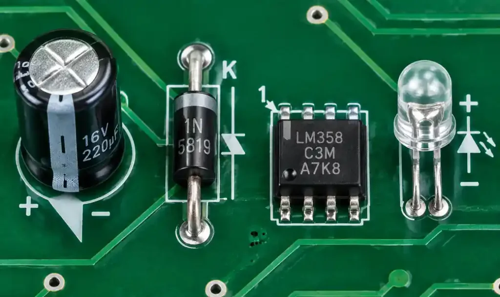
Polarity marks prevent reversed installation of diodes, electrolytic capacitors, LEDs, and polarized connectors. A single reversed electrolytic capacitor can destroy an entire circuit, making clear polarity indication critical.
For diodes and LEDs, add a filled triangle, bar, or “+” symbol at the cathode end. Make polarity marks at least 0.5mm long and 0.3mm from component edges.
Electrolytic capacitors require clear indication of the negative terminal. Print a filled wedge on the component outline’s negative side, matching the capacitor body’s white stripe orientation. Add a small “+” symbol on the positive side for redundancy—dual marking reduces installation errors from 8% to under 1%.
IC pin 1 indicators use a filled dot, chamfered corner, or notch in the component outline. Position the indicator 0.5mm outside the package corner where it remains visible even after component placement.
Connector orientation requires clear indication of pin 1 and keying direction. Add pin numbers at both ends of the connector outline with an arrow showing pin number progression.
Barcode and QR Code Integration
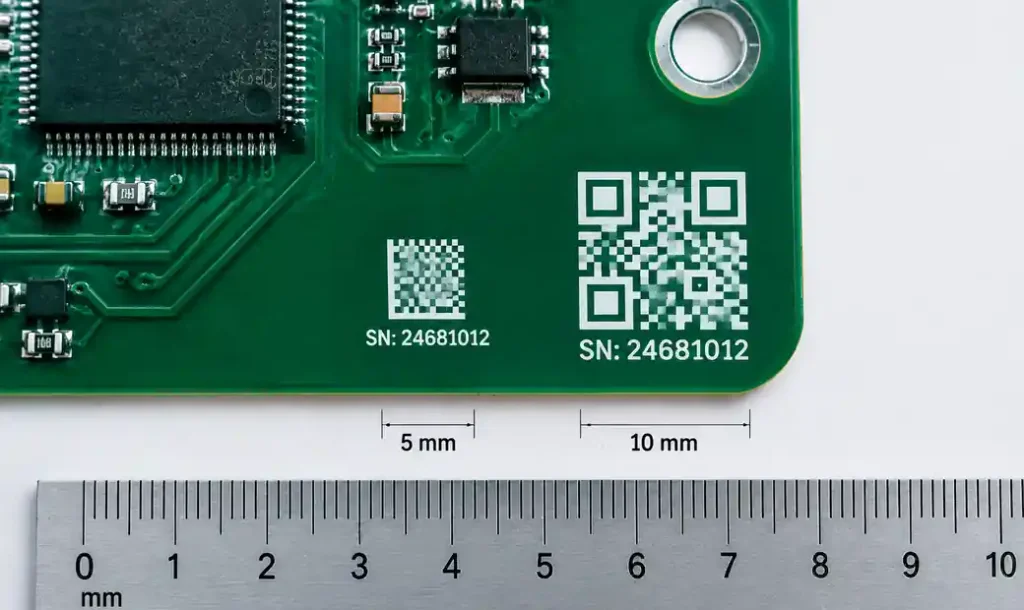
Automated inventory tracking requires machine-readable codes on PCBs. Data Matrix codes (2D barcodes) have become standard for electronics manufacturing because they encode more information in less space—a 5×5mm Data Matrix code stores a 15-character alphanumeric string.
Minimum cell size for Data Matrix codes is 0.30mm for screen printing and 0.20mm for LPI silkscreen. Use “Size 18” (18×18 cells) or larger for production codes; smaller sizes require LPI and controlled lighting for scanning.
Place codes in board corners or along edges where they won’t be covered by components. Position codes at least 5mm from board edges to prevent damage during depaneling. Add a 2-3mm quiet zone (blank area) around codes—scanners require this clear border.
QR codes work for larger boards where 10×10mm space is available. Standard QR codes use 0.50mm cell size and encode 50+ characters including web URLs. However, Data Matrix codes are preferred for small boards because they achieve equivalent data density in 60% less space.
Always print a human-readable backup (serial number or part number) adjacent to machine-readable codes.
Common Silkscreen Design Mistakes
Text overlapping solder pads represents the most frequent silkscreen error. Text touching pads may wick solder during reflow, creating bridges or poor joints. Set your DRC rules to enforce minimum 0.2mm clearance between silkscreen and all pad surfaces.
Silkscreen on via pads causes print defects and may plug via holes. Configure your CAD tool to automatically remove silkscreen from via pad areas.
Component outlines that don’t match actual part dimensions mislead assembly operators. Maintain accurate component library footprints with outlines matching installed component body dimensions within ±0.2mm.
Insufficient clearance between silkscreen and board edges causes text to be clipped during routing. Position text at least 1.5mm from board edges.
Using decorative fonts or italics reduces readability. Stick to simple sans-serif fonts with uniform stroke width.
Optimizing Silkscreen for Automated Assembly
SMT pick-and-place machines use vision systems that reference component outlines and fiducial marks. Clear component outlines assist operators during machine setup and manual correction of placement errors.
Fiducial marks require 2-3mm diameter circles with 0.15mm stroke width, placed in opposite corners of the board. Add a third fiducial for boards over 100mm in any dimension. Fiducials should be bare copper (no solder mask), but adding a silkscreen outline helps operators verify fiducial presence.
Test point identification accelerates ICT and flying probe testing. Add “TP” labels with sequential numbers (TP1, TP2…) adjacent to test pads, positioned where they’re visible with the test fixture in place.
Panel identification for multi-up designs requires unique markings on each board image. Add sequential numbers or alphanumeric codes to identify individual boards within the panel during assembly and testing.
FAQs
What is the absolute minimum silkscreen text size that will print reliably?
Standard screen printing requires 1.0mm (40 mils) character height with 0.15mm (6 mils) stroke width. LPI silkscreen can achieve 0.7mm height with 0.10mm strokes, but costs more and requires confirming your manufacturer supports this process. Text below these minimums may not print or will be illegible.
Can I use different silkscreen colors on the same board?
Yes, but each additional color requires a separate printing pass, adding cost and lead time. Multi-color silkscreen is typically reserved for high-end consumer products or safety-critical markings. Most manufacturers offer two-color silkscreen at 30-50% premium over single color.
Should silkscreen go on top layer only, or both sides?
Both sides if you have components on both sides. Bottom-side silkscreen helps during rework and field service when technicians need to identify components without flipping the board constantly. Single-sided assembly only requires top-side silkscreen.
How do I handle silkscreen for very dense designs with no space between components?
Use smaller LPI silkscreen (0.8mm height), abbreviate reference designators (R1 instead of RES1), omit component values, or print designators on internal silkscreen layers that appear only in assembly drawings. Accept that some ultra-dense areas may have minimal markings.
What information must appear in silkscreen for certification and compliance?
UL and CE marks, FCC ID numbers, patent numbers, and date codes are common regulatory requirements. Check specific regulations for your product category—medical devices (IEC 60601) and automotive (IATF 16949) have additional marking requirements.
Does silkscreen affect electrical performance or impedance?
No. Silkscreen is non-conductive epoxy ink with no electrical impact. However, avoid printing silkscreen over high-frequency transmission lines above 10 GHz—the dielectric constant of ink (approximately 3.5) slightly affects field distribution, potentially shifting impedance by 0.5-1 ohm.
Conclusion
Effective silkscreen design requires balancing readability, space constraints, and manufacturing capabilities. Following minimum text dimensions of 1.0-1.2mm height with 0.15-0.20mm stroke width ensures reliable printing. White ink on green solder mask provides optimal contrast, while consistent reference designator placement and clear polarity marks prevent assembly errors.
Integrate Data Matrix codes for traceability, maintain 0.2mm clearance from pads and board edges, and verify your manufacturer supports your specified silkscreen process before finalizing designs. Clear silkscreen reduces assembly time, lowers error rates, and simplifies troubleshooting.
For PCB manufacturing services with precision silkscreen capabilities including LPI and multi-color printing, Andwin Circuits provides prototypes and production volumes with full IPC-6012 compliance and automated optical inspection.