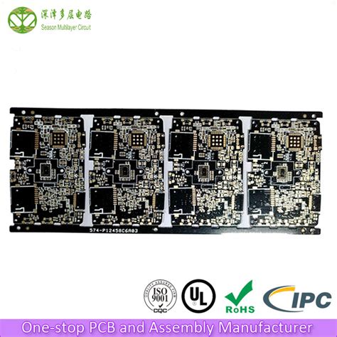
PCB Delamination: Causes, Effects, and Solutions
Introduction
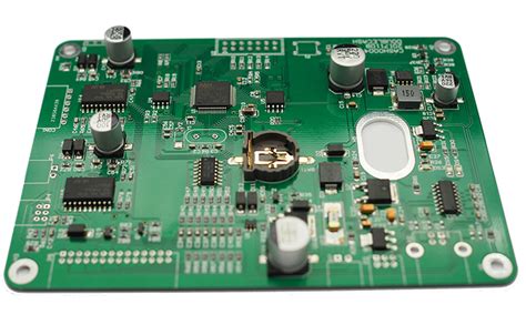
Printed Circuit Boards (PCBs) are essential components in modern electronics, serving as the foundation for electrical connections in devices ranging from smartphones to industrial machinery. However, one of the most critical reliability issues affecting PCBs is delamination—the separation of layers within the board. Delamination can lead to catastrophic failures, increased costs, and reduced product lifespan.
This article explores the causes, effects, detection methods, and solutions for PCB delamination, providing insights for engineers, manufacturers, and quality assurance professionals.
1. What is PCB Delamination?
Delamination refers to the separation of the PCB’s layers due to the breakdown of the adhesive bonds between the substrate, copper layers, and prepreg (pre-impregnated composite fibers). This can occur between:
- Copper and substrate
- Prepreg layers
- Solder mask and copper traces
When delamination happens, it compromises the structural integrity and electrical performance of the PCB, leading to potential failures.
2. Causes of PCB Delamination
2.1. Moisture Absorption
PCBs are hygroscopic, meaning they absorb moisture from the environment. If a PCB is exposed to high humidity before assembly, trapped moisture can vaporize during soldering (especially in reflow or wave soldering), creating internal pressure that causes layer separation.
2.2. Poor Material Quality
Low-quality base materials (e.g., FR-4 with impurities or inconsistent resin content) can weaken the bond between layers, increasing delamination risk.
2.3. Thermal Stress
- Excessive reflow temperatures can degrade the resin, weakening adhesion.
- Thermal cycling (repeated heating/cooling) causes expansion and contraction, leading to micro-cracks and eventual delamination.
2.4. Mechanical Stress
- Drilling and routing processes can introduce micro-fractures.
- Flexing or bending of rigid PCBs can weaken layer bonds.
2.5. Chemical Contamination
- Residual flux or cleaning agents can attack the laminate over time.
- Harsh chemical exposure during manufacturing (e.g., etching) may degrade adhesives.
2.6. Improper Lamination Process
- Insufficient pressure or temperature during lamination can result in weak bonding.
- Uneven resin distribution leads to weak spots.
3. Effects of PCB Delamination
3.1. Electrical Failures
- Open circuits due to broken copper traces.
- Short circuits if separated layers create unintended conductive paths.
- Increased resistance, leading to signal degradation.
3.2. Reduced Mechanical Strength
- Delaminated boards are more prone to cracking under stress.
- Component mounting becomes unreliable.
3.3. Thermal Management Issues
- Air gaps from delamination reduce heat dissipation, leading to overheating.
3.4. Long-Term Reliability Concerns
- Delamination can propagate over time, causing intermittent failures that are difficult to diagnose.
4. Detection and Testing Methods
4.1. Visual Inspection
- Blisters or bubbles on the PCB surface.
- Discoloration indicating moisture or chemical damage.
4.2. Microsectioning (Cross-Sectional Analysis)
- Cutting and examining PCB layers under a microscope to detect internal separations.
4.3. Thermal Stress Testing
- Thermal cycling tests simulate real-world conditions to identify weak points.
- Solder reflow simulation checks for moisture-induced delamination (popcorning).
4.4. Acoustic Microscopy (Scanning Acoustic Microscopy – SAM)
- Uses ultrasonic waves to detect voids or separations between layers.
4.5. Electrical Testing
- Impedance testing to detect changes caused by delamination.
- Continuity checks to find broken connections.
5. Solutions and Prevention Strategies
5.1. Proper Material Selection
- Use high-Tg (glass transition temperature) materials for high-temperature applications.
- Choose moisture-resistant laminates (e.g., polyimide for flexible PCBs).
5.2. Controlled Manufacturing Environment
- Store PCBs in moisture-controlled environments (<30% RH).
- Pre-bake PCBs before assembly to remove absorbed moisture.
5.3. Optimized Lamination Process
- Ensure proper temperature, pressure, and curing time during lamination.
- Use vacuum lamination to eliminate air pockets.
5.4. Improved Thermal Management
- Design PCBs with even heat distribution.
- Use thermal vias and heat sinks to minimize thermal stress.
5.5. Stress Relief in Design
- Avoid sharp corners in copper traces to reduce mechanical stress.
- Use flexible PCBs for applications requiring bending.
5.6. Post-Manufacturing Protection
- Apply conformal coatings to prevent moisture ingress.
- Use underfill for BGA components to reinforce solder joints.
6. Case Study: Delamination in Automotive Electronics
A leading automotive manufacturer faced PCB failures in engine control units (ECUs) due to delamination. Root cause analysis revealed:
- Moisture absorption during storage.
- Excessive thermal stress from engine heat.
Solution:
- Implemented moisture-proof packaging with desiccants.
- Switched to high-Tg laminates.
- Added pre-baking before assembly.
Result: Failure rate reduced by 85%.
7. Conclusion
PCB delamination is a critical issue that affects performance, reliability, and longevity. By understanding its causes—moisture, thermal stress, poor materials, and manufacturing defects—engineers can implement preventive measures such as proper material selection, controlled storage, optimized lamination, and robust testing.
As PCBs continue to evolve with higher density and more complex designs, addressing delamination proactively will remain essential for ensuring product reliability in industries ranging from consumer electronics to aerospace.
Key Takeaways:
✅ Moisture control is critical to preventing delamination.
✅ High-quality materials and proper lamination processes improve reliability.
✅ Thermal and mechanical stress must be managed in design and assembly.
✅ Advanced testing methods (SAM, cross-sectioning) help detect early signs of delamination.
By following best practices, manufacturers can minimize delamination risks and produce more durable, high-performance PCBs.