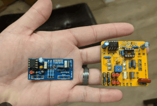
PCB Design and Assembly: Optimizing Efficiency and Reliability
Key Takeaways
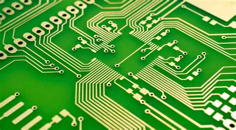
Effective PCB assembly requires a holistic approach that balances technical precision with strategic planning. Central to this process is layout optimization, which directly impacts signal integrity and thermal performance. Component selection plays a dual role: choosing high-reliability parts minimizes failure rates, while aligning with PCBA (Printed Circuit Board Assembly) standards ensures compatibility with automated manufacturing systems.
"A well-executed design-for-manufacturing (DFM) strategy can reduce assembly errors by 40% and accelerate time-to-market," notes industry veteran Dr. Elena Torres.
To maintain quality, consider these critical factors:
| Aspect | Traditional Approach | Advanced Technique |
|---|---|---|
| Component Placement | Manual alignment | Machine-learning-driven AOI |
| Testing | Sample-based inspection | Real-time impedance analysis |
| Thermal Management | Heatsinks & fans | Embedded copper pours |
Adopting AI-driven PCB design optimization allows engineers to simulate multiple scenarios, identifying potential signal interference or thermal hotspots before prototyping. For PCBA stages, prioritize:
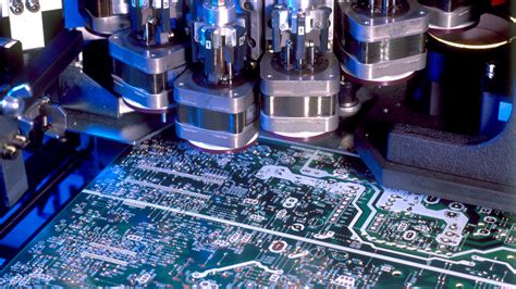
- Automated optical inspection (AOI) systems for micron-level defect detection
- Impedance-controlled routing to maintain signal integrity in high-frequency designs
- Via-in-pad technology for dense component layouts
Transitioning between design and production phases demands rigorous adherence to IPC-A-610 standards, particularly for solder joint quality and component spacing. This systematic approach not only enhances reliability but also streamlines the PCB assembly workflow across complex projects.
PCB Layout Optimization Techniques
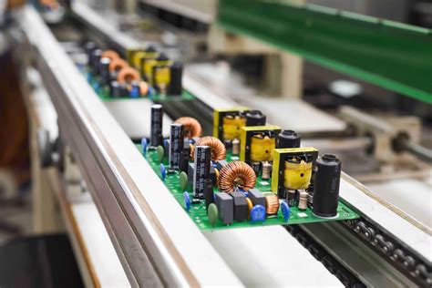
Effective PCB layout optimization begins with strategic trace routing, where minimizing path lengths between high-speed components reduces signal delay and electromagnetic interference. Grouping related circuits, such as power supply modules or analog signal chains, enhances PCB assembly efficiency by simplifying solder mask application and component placement. For PCBA reliability, maintain adequate clearance between heat-generating components and sensitive devices, using thermal vias or copper pours to dissipate energy effectively.
Another critical aspect involves optimizing pad geometries for surface-mount devices (SMDs), ensuring compatibility with automated pick-and-place systems during PCB assembly. Implementing balanced copper distribution across layers prevents warping during reflow soldering, a common issue in high-density PCBA designs. Additionally, adhering to Design for Manufacturability (DFM) guidelines—such as avoiding acute angles in traces—streamlines production and reduces defect rates.
By integrating simulation tools to analyze signal integrity and thermal behavior early in the design phase, engineers can preemptively address bottlenecks, aligning layouts with PCBA requirements for seamless transitions to manufacturing. This proactive approach not only accelerates prototyping but also strengthens long-term reliability in demanding environments.
Component Selection for PCB Reliability
Beyond layout considerations, the choice of components directly impacts the long-term performance and durability of PCB assembly outcomes. Critical parameters such as operating temperature ranges, voltage ratings, and environmental certifications (e.g., AEC-Q200 for automotive applications) must align with the end-use environment to prevent premature failures. For high-reliability PCBA projects, prioritizing components with proven mean time between failures (MTBF) data and robust supply chain availability reduces risks of field malfunctions or production delays.
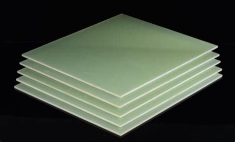
Thermal compatibility between components and the substrate material is equally vital—mismatched coefficients of thermal expansion (CTE) can induce mechanical stress during PCB assembly reflow processes or operational cycling. Implementing derating strategies for capacitors, connectors, and ICs further enhances resilience against voltage spikes or current overloads. When selecting surface-mount devices (SMDs), consider their compatibility with automated PCBA placement systems to minimize soldering defects. By balancing performance specifications, manufacturability, and lifecycle demands, designers create boards that withstand both assembly rigors and real-world operational challenges.

Ensuring Quality in PCB Assembly
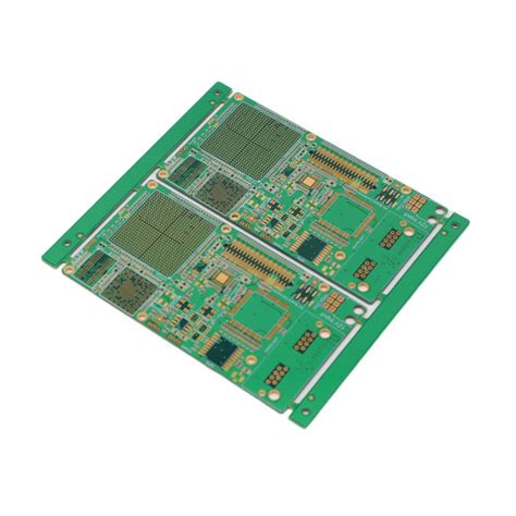
Maintaining rigorous quality standards during PCB assembly is critical to achieving reliable end products. The process begins with comprehensive inspection protocols, including automated optical inspection (AOI) and X-ray testing, to detect defects like soldering irregularities or component misalignment. Implementing statistical process control (SPC) methodologies ensures consistency across production batches by monitoring key parameters such as solder paste deposition accuracy and reflow oven temperature profiles.
Material selection plays a pivotal role in PCBA reliability. Using high-grade substrates and solder alloys with low thermal expansion coefficients minimizes stress-induced failures. Additionally, traceability systems track components from procurement to final assembly, mitigating risks from counterfeit parts. For complex designs, design-for-manufacturability (DFM) reviews align layout choices with assembly capabilities, reducing rework rates.
Post-assembly, functional testing validates electrical performance under simulated operating conditions. Environmental stress screening (ESS), including thermal cycling and vibration tests, identifies latent defects before deployment. By integrating these practices, manufacturers ensure PCB assembly processes meet industry benchmarks like IPC-A-610, balancing efficiency with uncompromised quality.

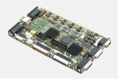
Advanced Techniques in PCB Assembly
Innovations in PCB assembly processes are redefining manufacturing precision and reliability. One key advancement is the adoption of automated optical inspection (AOI) systems, which detect microscopic defects in solder joints or misaligned components during PCBA production. Pairing this with inline X-ray inspection (AXI) ensures hidden faults, such as voids in ball grid arrays (BGAs), are identified early. Manufacturers are also leveraging laser-assisted depaneling to reduce mechanical stress on boards, preserving circuit integrity in high-density designs.
Another transformative approach involves integrating 3D printing for rapid prototyping of custom jigs and fixtures, streamlining the PCB assembly workflow. For high-frequency applications, controlled impedance routing and sequential lamination techniques minimize signal loss, while vacuum reflow ovens enhance solder joint uniformity in complex PCBA configurations. Additionally, predictive maintenance algorithms applied to pick-and-place machinery reduce downtime by anticipating wear in critical components like nozzles or feeders.
To address miniaturization challenges, microvia-in-pad designs and advanced underfill materials are being deployed to strengthen connections in ultra-thin packages. These methods, combined with real-time traceability systems, ensure compliance with stringent industry standards. By harmonizing these innovations, manufacturers achieve faster turnaround times without compromising the durability or performance of assembled boards.
Thermal Management in PCB Design
Effective thermal management is critical for ensuring the longevity and reliability of PCB assembly (PCBA) in high-performance applications. As component density increases and power demands grow, heat dissipation becomes a pivotal factor in preventing premature failure. Strategic placement of thermal vias and copper pours helps distribute heat evenly across the board, minimizing hotspots that could degrade solder joints or damage sensitive components.
Material selection plays a key role here: using substrates with higher thermal conductivity, such as metal-core or ceramic-based laminates, enhances heat transfer. Additionally, integrating heatsinks or thermally conductive pads in the PCBA layout ensures efficient cooling for power-intensive components like voltage regulators or processors.
Designers must also account for airflow dynamics in the final product enclosure. Aligning high-heat areas with ventilation paths and avoiding obstructions in the PCB assembly stack-up can significantly improve thermal performance. Advanced simulation tools, such as finite element analysis (FEA), enable precise modeling of heat distribution, allowing iterative adjustments before prototyping.
By balancing these strategies, engineers achieve optimal thermal stability, which directly impacts the reliability of the PCBA in demanding environments—from automotive systems to industrial automation. This proactive approach not only extends product lifespan but also reduces warranty claims and field failures.
Implementing DFM in PCB Design
Integrating Design for Manufacturability (DFM) principles early in the PCB design process ensures seamless transition to PCB assembly while minimizing costly revisions. By prioritizing manufacturing constraints during layout planning, designers can avoid common pitfalls such as insufficient component spacing, impractical trace widths, or incompatible pad geometries. For instance, aligning drill hole sizes with standard PCBA tooling specifications reduces fabrication delays and improves yield rates. Collaboration between design engineers and assembly partners is critical to identify thermal management requirements, material compatibility, and testing access points upfront. Modern software tools now automate DFM checks, flagging issues like solder mask slivers or uneven copper distribution that could compromise reliability. Additionally, optimizing panelization layouts for PCB assembly workflows—such as balancing component density or incorporating fiducial markers—streamlines mass production. Addressing coefficient of thermal expansion (CTE) mismatches between substrates and components further enhances durability in high-stress environments. By embedding DFM practices, teams not only accelerate time-to-market but also ensure that designs meet stringent quality benchmarks required for mission-critical applications.
AI-Driven PCB Design Optimization
Integrating artificial intelligence into PCB design processes is revolutionizing how engineers approach layout optimization and pcb assembly workflows. Machine learning algorithms analyze vast datasets of historical designs, identifying patterns to recommend component placement strategies that minimize signal interference and reduce thermal stress. These AI tools automatically adjust trace routing to optimize impedance matching, a critical factor for high-frequency pcba performance. By simulating thousands of manufacturing scenarios, predictive models highlight potential failure points in solder joints or component alignment before physical prototyping.
Advanced AI platforms now incorporate real-time collaboration between design and pcb assembly teams, dynamically updating layouts based on material availability or manufacturing constraints. For instance, neural networks trained on solder paste inspection data can predict stencil printing defects, enabling preemptive corrections during the pcba phase. This synergy between algorithmic precision and pcb assembly expertise reduces iteration cycles by 30–40% while improving first-pass yield rates. Crucially, AI-driven thermal analysis tools map heat dissipation pathways across multilayer boards, ensuring reliability without compromising component density—a balance previously achievable only through extensive trial and error.
PCB Testing for Quality Assurance
Thorough testing protocols are critical for ensuring the reliability of PCB assembly processes. Modern PCBA (printed circuit board assembly) workflows employ a multi-layered approach to quality assurance, combining automated optical inspection (AOI), in-circuit testing (ICT), and functional validation. AOI systems use high-resolution cameras to detect soldering defects, misaligned components, or trace irregularities, while ICT verifies electrical connectivity and component functionality under simulated operating conditions.
For complex designs, X-ray inspection becomes indispensable, revealing hidden flaws like voids in ball grid array (BGA) solder joints or internal layer misregistrations. Advanced PCB assembly providers also integrate environmental stress testing—such as thermal cycling and vibration tests—to mimic real-world operating challenges. These evaluations ensure that the final PCBA can withstand temperature fluctuations, mechanical shocks, and prolonged usage without performance degradation.
By aligning testing methodologies with design-for-manufacturability (DFM) principles, engineers reduce the risk of post-production failures. Real-time data analytics further enhance defect detection accuracy, enabling rapid corrections during the PCB assembly phase. This systematic approach not only minimizes rework costs but also strengthens the end product’s compliance with industry standards like IPC-A-610.
Conclusion
The integration of PCB design and pcb assembly processes forms the backbone of modern electronics manufacturing, where efficiency and reliability are non-negotiable. By aligning design intent with manufacturing capabilities, engineers can mitigate risks such as component misalignment or thermal stress, ensuring seamless transitions from prototyping to mass production. A collaborative approach between design teams and pcba specialists enables the implementation of Design for Manufacturability (DFM) principles, reducing rework and accelerating time-to-market.
Advanced tools like AI-driven simulations and automated optical inspection (AOI) further refine pcb assembly accuracy, while rigorous testing protocols validate performance under real-world conditions. As technologies evolve, prioritizing material compatibility and supply chain resilience remains critical to sustaining long-term reliability. Ultimately, the synergy between innovative design strategies and precision-driven pcba workflows not only optimizes product longevity but also positions organizations to adapt swiftly to emerging industry demands. Continuous improvement in these areas ensures that both current and future electronic systems meet escalating expectations for functionality and durability.
FAQs
How does layout optimization impact PCB reliability?
Proper layout optimization minimizes signal interference and improves thermal distribution, directly enhancing the longevity of PCB assembly. Strategic trace routing and component placement reduce electromagnetic interference (EMI), ensuring stable performance in PCBA applications.
What criteria should guide component selection for reliability?
Prioritize components with temperature tolerance and certification compliance. High-quality materials withstand environmental stress, while standardized footprints simplify PCB assembly processes. Always verify supplier credentials to avoid counterfeit parts in PCBA workflows.
Why is Design for Manufacturability (DFM) critical?
DFM principles bridge design and production, eliminating errors that cause delays. By aligning with PCB assembly capabilities early, designers avoid mismatches in pad sizes or layer stack-ups, streamlining PCBA timelines and reducing costs.
How do thermal management techniques affect performance?
Effective heat dissipation through copper pours or thermal vias prevents overheating, which can degrade components. This is especially vital in high-density PCBA designs, where localized heat buildup risks circuit integrity.
What role does testing play in quality assurance?
Automated optical inspection (AOI) and functional testing identify defects like solder bridges or open circuits. Rigorous testing protocols ensure every PCB assembly meets performance benchmarks before deployment.
Explore Professional PCB Assembly Solutions
For tailored PCB assembly services that prioritize efficiency and reliability, please click here to connect with industry experts.