PCB Design-Fabrication-Assembly: Best Practices
Key Takeaways
Effective PCB assembly (PCBA) requires harmonizing design intent with manufacturing realities. Three critical focus areas emerge:
- Design-for-Manufacturing (DFM) principles minimize rework by addressing tolerances, component spacing, and thermal management during layout stages.
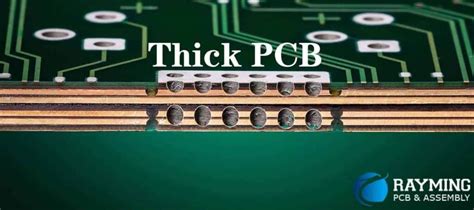
- Fabrication-process synchronization ensures materials (e.g., FR-4 substrates) and layer stackups align with PCBA requirements for signal integrity.
- Automated optical inspection (AOI) systems in assembly lines reduce defects by 40–60% compared to manual checks.
"Always validate solder mask clearances against your contract manufacturer’s capabilities before finalizing designs." – Industry QC Specialist
| Consideration | Traditional Approach | Optimized Approach |
|---|---|---|
| Component Placement | Manual adjustments during PCB assembly | DFM-driven automated placement |
| Thermal Management | Post-design heat sinks | Embedded copper pours + thermal vias |
| Testing | End-of-line functional tests | In-process AOI + boundary scan |
For PCBA success, prioritize cross-functional collaboration between design and production teams. Implement traceability systems to track fabrication parameters (e.g., etching times, lamination pressures) back to assembly outcomes. This data-driven method cuts troubleshooting time by 35% while improving yield rates.
PCB Design Optimization Techniques
Effective PCB design optimization begins with understanding the interplay between electrical performance, manufacturability, and PCBA (printed circuit board assembly) requirements. Prioritizing design for manufacturability (DFM) principles ensures seamless transitions from design to PCB fabrication and assembly. Critical steps include optimizing component placement to minimize signal interference, selecting trace widths that balance current capacity and space constraints, and implementing thermal management strategies such as copper pours or heatsinks.
Leveraging automated design tools for routing and layer stack-up planning reduces errors while adhering to PCB assembly tolerances. For instance, maintaining proper clearance between high-voltage components and low-power circuits prevents arcing risks during PCBA. Additionally, incorporating test points early in the design phase simplifies post-assembly diagnostics.
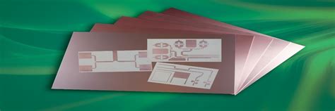
Material selection also plays a pivotal role—choosing substrates with appropriate dielectric constants or thermal expansion coefficients enhances reliability in demanding environments. By aligning design choices with fabrication capabilities—such as avoiding excessively thin traces for cost-sensitive projects—teams can mitigate delays and rework. Finally, validating designs through simulation tools like signal integrity analysis ensures compliance with performance benchmarks before committing to production.
Streamlining PCB Fabrication Processes
Efficient PCB fabrication requires harmonizing precision with scalability. A critical step involves optimizing design-for-manufacturing (DFM) principles to eliminate errors early, reducing rework and material waste. Modern fabrication facilities leverage automated optical inspection (AOI) systems to detect microscopic defects in copper traces or solder masks, ensuring consistency across high-volume production runs.
Transitioning from design to fabrication demands close collaboration between engineers and manufacturers. For instance, adjusting trace widths or layer stack-ups to align with pcb assembly tolerances can prevent mismatches during PCBA integration. Advanced techniques like laser direct imaging (LDI) enhance pattern accuracy, particularly for high-density interconnect (HDI) boards, while panelization strategies maximize material utilization.
To further streamline workflows, real-time data analytics monitor equipment performance and process variables, such as etching rates or lamination temperatures. This proactive approach minimizes downtime and ensures adherence to tight tolerances. Additionally, adopting standardized protocols like IPC-6012 for reliability testing bridges fabrication and pcb assembly, creating a seamless transition to final PCBA stages.
By integrating these practices, manufacturers achieve faster turnaround times without compromising quality—a vital balance for industries ranging from consumer electronics to aerospace.
Effective PCB Assembly Strategies
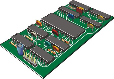
Successful PCB assembly requires meticulous coordination between design specifications and manufacturing capabilities. Implementing design for manufacturability (DFM) principles early reduces errors during PCBA (printed circuit board assembly), ensuring components align with fabrication tolerances. Prioritize component selection by verifying availability and compatibility with automated placement systems, minimizing delays caused by obsolete or mismatched parts.
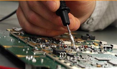
Automated optical inspection (AOI) and X-ray testing should follow solder paste application and reflow processes to detect defects like bridging or cold joints. For mixed-technology boards, combine surface-mount (SMT) and through-hole (THT) techniques, adjusting reflow profiles to prevent thermal damage to sensitive ICs. Proper stencil design—optimizing aperture ratios and alignment—ensures consistent solder deposition, critical for fine-pitch components.
Collaboration with fabrication partners is essential; reviewing PCB fabrication guidelines helps align material choices with assembly requirements, such as Tg ratings for high-temperature applications. Finally, functional testing validates PCBA performance under real-world conditions, addressing signal integrity or power delivery issues before mass production. By integrating these strategies, manufacturers achieve higher yield rates while maintaining cost and timeline efficiency.
Integrating PCB Design-Fabrication-Assembly
Seamless integration of PCB design, fabrication, and pcb assembly (PCBA) is critical for achieving functional, cost-effective electronics. While each stage operates independently in traditional workflows, modern practices emphasize concurrent engineering to bridge gaps between design intent and manufacturing realities. Designers must prioritize Design for Manufacturability (DFM) principles, such as optimizing trace widths and component spacing, to avoid fabrication bottlenecks. Similarly, Design for Assembly (DFA) considerations—like standardized footprints and automated placement compatibility—streamline PCBA processes.
Transitioning from design to production requires iterative prototyping to validate thermal management, signal integrity, and mechanical fit. For instance, impedance-controlled routing in high-frequency designs demands precise material selection during fabrication, which directly impacts solderability in pcb assembly. Collaborative tools like 3D PCB mockups and real-time feedback loops between design teams and manufacturers help identify conflicts early, reducing rework. By aligning PCB design rules with fabrication tolerances and PCBA capabilities, teams can accelerate time-to-market while maintaining rigorous quality standards—a foundation for the subsequent discussion on quality control protocols.
Quality Control in PCB Manufacturing
Effective quality control in PCB manufacturing ensures reliability across design, fabrication, and PCB assembly stages. Automated optical inspection (AOI) systems scan PCBA layers for defects like misaligned traces or solder bridges, while X-ray imaging verifies internal connections in multilayer boards. Statistical process control (SPC) tools monitor production metrics, such as copper thickness and hole drilling accuracy, to maintain tolerances within ±5%.
During PCB assembly, solder paste inspection (SPI) systems validate stencil printing consistency, reducing rework risks. Functional testing post-assembly simulates real-world conditions to detect latent failures, with environmental stress screening (ESS) exposing boards to thermal cycling and vibration. Manufacturers also enforce material traceability, documenting PCBA component origins to comply with ISO 9001 or IPC-A-610 standards.
By integrating these protocols early in the production chain, defects are minimized before reaching final validation. This alignment between PCB fabrication and assembly not only reduces scrap rates but also ensures end products meet performance benchmarks critical for aerospace, medical, and automotive applications.
Avoiding Common PCB Design Mistakes
Preventing costly errors in PCB assembly begins with addressing fundamental design oversights. A frequent misstep involves inadequate clearance between components and board edges, which can compromise PCBA reliability during automated placement. Designers must also verify thermal management strategies, as improper heat dissipation paths often lead to premature failure in high-density layouts. Another critical area is footprint accuracy—mismatched component libraries cause alignment issues in PCB assembly, resulting in rework delays.
Transitioning from design to production requires meticulous attention to manufacturing tolerances. Failing to account for fab house capabilities—such as minimum trace widths or drill sizes—can derail PCBA timelines. Additionally, overlooking test point accessibility complicates quality assurance, increasing post-assembly inspection costs. To maintain coherence with fabrication and assembly phases, designers should implement design rule checks (DRCs) that align with both PCB assembly workflows and end-product requirements.
Finally, silkscreen errors—like reversed polarity indicators or ambiguous labels—create avoidable confusion during PCBA processes. Adopting standardized symbol libraries and cross-referencing BOMs with layout files minimizes these risks. By integrating fabrication and PCB assembly constraints early, designers mitigate re-spins and ensure seamless transitions between development stages.
Cost-Effective PCB Manufacturing Solutions
Achieving cost efficiency in PCB manufacturing requires strategic alignment between design, pcb assembly, and material selection. Start by optimizing panelization layouts to minimize material waste during fabrication—a practice that reduces raw material costs by up to 15%. Leveraging Design for Manufacturability (DFM) principles early in the design phase ensures compatibility with automated pcba workflows, lowering labor expenses and rework risks.
Another critical aspect involves selecting standardized components over custom parts, which streamlines procurement and reduces lead times. For high-volume production, partnering with manufacturers offering bulk pricing for substrates or solder masks can yield significant savings. However, avoid compromising on quality for cost—hidden expenses from faulty boards or delayed deliveries often offset initial savings.
Modern pcb assembly lines benefit from automated pick-and-place systems and reflow ovens, which enhance precision while cutting assembly time. For pcba projects, consider hybrid manufacturing models that combine automated processes with selective manual inspection for critical components. Finally, implementing real-time quality checks during fabrication and assembly phases prevents costly defects from progressing downstream, ensuring both affordability and reliability in the final product.
Ensuring Reliability in PCB Production
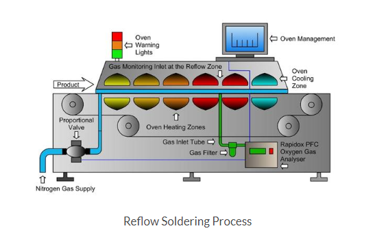
Achieving consistent reliability in PCB production requires rigorous adherence to design-for-manufacturing (DFM) principles and robust quality assurance protocols. During PCB assembly (often abbreviated as PCBA), component placement accuracy and solder joint integrity become critical factors. Automated optical inspection (AOI) and X-ray testing are widely adopted to detect micro-defects, such as voids in ball grid arrays (BGAs) or misaligned surface-mount devices (SMDs). Thermal profiling during reflow soldering ensures optimal bonding without subjecting components to excessive thermal stress.
Material selection also plays a pivotal role. High-performance substrates with low dielectric loss and copper foils with controlled roughness minimize signal degradation in high-frequency applications. For PCBA workflows, using solder pastes with appropriate viscosity and alloy composition reduces the risk of cold joints or tombstoning. Additionally, environmental stress testing—including thermal cycling and humidity exposure—validates long-term durability under real-world conditions.
To maintain alignment with the broader PCB design-fabrication-assembly chain, manufacturers must enforce IPC-A-610 standards for acceptability and leverage statistical process control (SPC) to monitor production variations. Collaboration between design engineers and assembly teams early in the process helps identify potential failure points, such as inadequate clearances or incompatible component footprints, before they escalate into costly rework.
Conclusion
The integration of PCB design, fabrication, and pcb assembly forms a cohesive workflow that determines the success of electronic products. Optimizing each phase—from layout precision to material selection and PCBA (Printed Circuit Board Assembly) execution—ensures functional reliability and cost efficiency. By aligning design intent with manufacturing capabilities, teams mitigate risks like signal interference or thermal mismanagement, while streamlined fabrication processes reduce waste and lead times.
A critical best practice lies in fostering collaboration between design engineers and pcb assembly specialists early in development. This synergy enables proactive adjustments, such as adhering to Design for Manufacturability (DFM) guidelines or selecting surface-mount components compatible with automated PCBA lines. Rigorous quality control, including automated optical inspection (AOI) and functional testing, further safeguards against defects in high-volume production.
Ultimately, mastering this triad demands continuous learning and adaptation to emerging technologies—whether in high-density interconnect (HDI) designs or eco-friendly fabrication methods. By prioritizing precision, scalability, and cross-functional communication, businesses can deliver robust, market-ready solutions that meet evolving industry standards.
Frequently Asked Questions
What distinguishes PCB fabrication from PCB assembly?
PCB fabrication refers to creating the bare board through etching copper layers and laminating materials, while PCB assembly (PCBA) involves populating the board with components like resistors and ICs. Both stages require precise coordination to ensure design intent translates into functional electronics.
How can design errors impact PCBA efficiency?
Flaws in pad sizing, component spacing, or silkscreen alignment often lead to assembly defects such as tombstoning or solder bridges. Implementing design for manufacturability (DFM) checks minimizes rework and accelerates PCBA timelines.
What quality controls are critical during PCB assembly?
Automated optical inspection (AOI), X-ray testing, and functional testing verify solder joint integrity and component placement accuracy. Combining these with thermal profiling ensures reliability in high-stress environments.
Why is material selection vital for PCBA longevity?
Substrates with low thermal expansion coefficients (e.g., FR-4) and lead-free solder alloys prevent delamination and cracking. This is especially crucial for boards exposed to temperature cycling or mechanical shocks.
Can prototyping reduce PCB assembly costs?
Yes. Prototyping identifies design-fabrication mismatches early, avoiding bulk-order defects. Many manufacturers offer turnkey PCBA services that streamline prototyping-to-production transitions.
Explore Professional PCB Assembly Solutions
For tailored PCB assembly expertise and end-to-end project support, please click here to connect with industry-leading specialists.