PCB Design for AC and DC Circuits: Key Considerations and Best Practices
Introduction to AC and DC PCB Design
Printed Circuit Board (PCB) design forms the foundation of modern electronics, serving as the physical platform that connects and supports various electronic components. When designing PCBs for circuits involving alternating current (AC) and direct current (DC), engineers face unique challenges that require specialized knowledge and careful consideration.
AC (Alternating Current) and DC (Direct Current) represent the two fundamental types of electrical power in electronic systems. AC periodically changes direction, typically following a sinusoidal waveform at specific frequencies (50Hz or 60Hz for mains power, higher frequencies for signals). DC flows consistently in one direction, providing stable voltage levels essential for digital circuits and most electronic components.
The design considerations for AC and DC circuits on PCBs differ significantly due to their distinct electrical characteristics. AC circuits demand special attention to impedance matching, noise reduction, and electromagnetic interference (EMI), while DC circuits focus more on stable voltage distribution, proper decoupling, and minimizing voltage drops. Mixed-signal designs that incorporate both AC and DC elements present additional challenges in maintaining signal integrity while preventing cross-talk between different circuit sections.
This article explores the essential aspects of PCB design for AC and DC applications, covering fundamental concepts, layout strategies, component selection, and advanced techniques to optimize performance and reliability in both domains.
Fundamental Differences in AC and DC PCB Design
Current Flow Characteristics
The primary distinction between AC and DC PCB design stems from their current flow characteristics. In DC circuits, current maintains a constant direction, resulting in steady electromagnetic fields around conductors. This stability simplifies many design aspects, as engineers primarily need to ensure proper voltage levels and adequate current-carrying capacity.
AC circuits, by contrast, feature continuously alternating current that creates time-varying electromagnetic fields. These dynamic fields introduce several complications:
- Skin Effect: At higher frequencies, AC current tends to flow near the conductor’s surface rather than uniformly throughout the cross-section. This effect increases effective resistance and must be considered in trace width calculations.
- Proximity Effect: Nearby conductors carrying AC currents influence each other’s current distribution, potentially increasing losses.
- Radiation: Alternating currents can radiate electromagnetic energy, potentially causing interference with other circuits or failing regulatory EMI requirements.
Impedance Considerations
While DC circuits primarily deal with resistance (R), AC circuits must account for impedance (Z), which combines resistance with reactance (X) from capacitive and inductive effects:
Z = √(R² + X²)
The reactive components introduce frequency-dependent behavior that significantly impacts PCB design:
- Capacitive Reactance (Xc): Decreases with frequency (Xc = 1/(2πfC))
- Inductive Reactance (XL): Increases with frequency (XL = 2πfL)
These relationships mean that trace geometries, dielectric materials, and component placements that work perfectly for DC may cause serious issues in AC circuits, especially at higher frequencies.
Signal Integrity Challenges
AC signals on PCBs face several integrity challenges that DC circuits typically avoid:
- Reflections: Impedance mismatches cause signal reflections that distort waveforms
- Crosstalk: Adjacent traces can capacitively or inductively couple, transferring unwanted signals
- Attenuation: High-frequency signals experience greater losses through the dielectric material
- Dispersion: Different frequency components travel at slightly different velocities
DC power distribution has its own challenges, primarily related to maintaining stable voltage levels across the entire board despite varying load conditions and parasitic resistances.
PCB Layout Strategies for AC Circuits
Trace Routing for AC Signals
Proper trace routing is critical for maintaining AC signal integrity:
- Impedance Control: Calculate and maintain consistent characteristic impedance for high-frequency traces. Use controlled impedance stackups with appropriate dielectric materials.
- Minimize Length: Keep AC signal traces as short as possible to reduce losses and susceptibility to interference.
- Avoid Sharp Corners: Use 45° angles or curved traces instead of 90° turns to prevent impedance discontinuities and radiation.
- Differential Pair Routing: For high-speed AC signals, route differential pairs with consistent spacing and length matching.
- Reference Planes: Provide uninterrupted reference planes (ground or power) beneath AC traces to control impedance and provide return paths.
Grounding Techniques for AC Circuits
Effective grounding is essential for AC circuit performance:
- Star Grounding: Connect all ground points to a single central location to prevent ground loops.
- Separate Analog and Digital Grounds: In mixed-signal designs, keep AC (analog) and DC (digital) ground systems separate, connecting them at a single point.
- Ground Plane Integrity: Maintain continuous ground planes beneath AC circuits, avoiding splits or slots that could disrupt return currents.
- RF Grounding: For radio frequency (RF) circuits, use multiple vias to connect to ground planes, reducing inductance.
EMI Reduction Techniques
AC circuits, especially those operating at high frequencies, can generate significant electromagnetic interference:
- Shielding: Use grounded copper pours or metal shields around sensitive AC circuits.
- Proper Filtering: Implement appropriate filters at AC inputs and outputs to suppress unwanted frequencies.
- Component Placement: Position potential noise sources away from sensitive AC circuits.
- Twisted Pair Routing: For board-to-board AC connections, consider using twisted pair cables to cancel magnetic fields.
DC Circuit Design Considerations
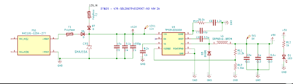
Power Distribution Network (PDN) Design
An effective PDN is crucial for reliable DC operation:
- Power Plane Design: Use dedicated power planes for major DC voltages to provide low-impedance distribution.
- Decoupling Capacitors: Place appropriate decoupling capacitors near IC power pins to suppress high-frequency noise.
- Voltage Regulator Placement: Position regulators close to their loads to minimize voltage drops.
- Current Capacity: Ensure traces and planes can handle maximum DC currents without excessive voltage drop or heating.
Thermal Management in DC Circuits
DC circuits often deal with significant power dissipation:
- Copper Weight: Use appropriate copper thickness (e.g., 2oz instead of 1oz) for high-current traces.
- Thermal Relief: Implement thermal relief patterns for component pads connected to large copper areas.
- Heat Sinking: Incorporate thermal vias and heatsinks for components with high power dissipation.
- Temperature Monitoring: Consider adding temperature sensors in areas prone to heating.
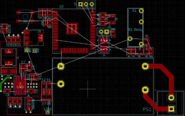
Mixed-Signal Layout Techniques
When combining AC and DC circuits on the same PCB:
- Partitioning: Physically separate AC and DC circuit sections on the board.
- Crossing Traces: Make AC and DC traces cross at right angles if they must intersect.
- Guard Traces: Place grounded guard traces between sensitive AC traces and noisy DC lines.
- Layer Stacking: Route AC signals on different layers than DC power, with ground planes between them.
Component Selection and Placement
Choosing Components for AC/DC Applications
- Capacitors: Select appropriate dielectric materials (NPO/C0G for AC coupling, X7R/X5R for decoupling).
- Inductors: Consider self-resonant frequency and current rating for AC applications.
- Resistors: Use film resistors for AC circuits where parasitic inductance matters.
- ICs: Verify frequency response and power requirements for both AC and DC characteristics.
Strategic Component Placement
- Signal Flow: Arrange components to maintain logical signal flow and minimize trace lengths.
- Power Sequencing: Position DC power components to support proper power-up sequencing.
- Noise Isolation: Place noisy components (switches, regulators) away from sensitive AC circuits.
- Accessibility: Consider test points and serviceability during placement.
Advanced Techniques and Future Trends
High-Frequency Design Considerations
As frequencies increase into the RF and microwave ranges:
- Transmission Line Theory: Treat all traces as transmission lines with careful impedance control.
- Material Selection: Use low-loss dielectric materials like Rogers laminates for critical high-frequency sections.
- Via Design: Optimize via structures to minimize impedance discontinuities.
- 3D EM Simulation: Utilize advanced simulation tools to predict and optimize high-frequency performance.
Power Integrity Analysis
Modern PCB design requires thorough power integrity analysis:
- DC Drop Analysis: Verify acceptable voltage levels at all load points.
- AC Impedance Analysis: Ensure power delivery network impedance meets target specifications across frequency spectrum.
- Decoupling Optimization: Use simulation to determine optimal decoupling capacitor values and placements.
Emerging Technologies
Future PCB design trends impacting AC/DC circuits:
- Embedded Components: Passive components integrated within the PCB layers.
- Advanced Materials: Graphene and other nanomaterials for improved conductivity and thermal performance.
- Additive Manufacturing: 3D printed electronics enabling novel circuit geometries.
- AI-Assisted Design: Machine learning algorithms optimizing layout for mixed-signal performance.
Conclusion
PCB design for AC and DC circuits demands a comprehensive understanding of electrical principles, material properties, and layout strategies. While DC circuit design focuses on stable power delivery and thermal management, AC circuit design emphasizes impedance control, signal integrity, and EMI reduction. Successful mixed-signal designs require careful partitioning, proper grounding, and strategic component placement to maintain the integrity of both AC and DC domains.
As electronic systems continue to evolve with higher frequencies and greater complexity, PCB designers must stay abreast of advanced techniques and emerging technologies. By applying the principles outlined in this article—from fundamental current flow considerations to advanced power integrity analysis—engineers can create robust, reliable PCBs that effectively support both AC and DC circuit requirements.
The future of PCB design lies in increasingly sophisticated simulation tools, novel materials, and innovative manufacturing techniques that will enable even more compact and efficient mixed-signal designs. However, the core principles of understanding current behavior, managing electromagnetic effects, and optimizing physical layouts will remain essential for creating successful AC/DC PCB designs.