PCB Design for LED and Touch Screen Displays: Key Considerations and Best Practices
Introduction
Printed Circuit Board (PCB) design forms the foundation of modern electronic displays, particularly for LED screens and touch screen interfaces. As these technologies become increasingly ubiquitous in consumer electronics, industrial equipment, and public information systems, the importance of optimized PCB design has never been greater. This article explores the critical aspects of PCB design specific to LED displays and touch screen technologies, covering layout considerations, material selection, signal integrity, power distribution, and manufacturing challenges.
Section 1: Fundamentals of Display PCB Design
1.1 Basic Architecture of Display PCBs
Display PCBs serve as the central nervous system of both LED and touch screen displays, responsible for power distribution, signal processing, and component control. The typical architecture includes:
- Power regulation circuits
- Controller/processor interfaces
- Driver ICs for LEDs or touch sensors
- Connector interfaces
- Signal conditioning components
1.2 Common PCB Stackups for Display Applications
Modern display PCBs often utilize multilayer designs to accommodate complex routing requirements:
- 4-layer stackup: Common for simpler LED displays
- Top Layer: Components and high-speed signals
- Inner Layer 1: Ground plane
- Inner Layer 2: Power plane
- Bottom Layer: Routing and components
- 6-8 layer stackup: Used for high-resolution displays and advanced touch screens
- Additional layers for signal isolation and impedance control
Section 2: LED Display PCB Design Considerations
2.1 LED Matrix Layout
The physical arrangement of LEDs on the PCB significantly impacts display quality:
- Pixel pitch determination based on viewing distance
- Grid vs. staggered layouts for different applications
- Thermal considerations for high-brightness LEDs
- Current distribution balancing across the array
2.2 Power Delivery Challenges
LED displays present unique power requirements:
- High current demands (especially for large outdoor displays)
- Voltage drop considerations across long traces
- Implementation of proper current limiting (resistors or constant-current drivers)
- Decoupling capacitor placement for stable operation
2.3 Thermal Management
Effective heat dissipation is critical for LED longevity:
- Copper pour techniques for heat spreading
- Thermal via arrays under high-power LEDs
- Material selection (high-Tg FR4 or metal-core PCBs)
- Considerations for forced air cooling in enclosure design
2.4 Signal Integrity in LED Drivers
Maintaining signal quality is essential for display performance:
- Proper grounding for PWM dimming signals
- Minimizing crosstalk between data lines
- Impedance control for high-speed serial interfaces (like SPI or LVDS)
- Shielding techniques for noise-sensitive analog sections
Section 3: Touch Screen PCB Design Considerations
3.1 Touch Sensor Technologies
Different touch technologies impose varying PCB requirements:
- Resistive touch: Simple interface but requires precise mechanical design
- Capacitive touch: More complex PCB layout with sensitive analog front-end
- Surface Acoustic Wave: Specialized transducer design
- Infrared: Precise optoelectronic component placement
3.2 Capacitive Touch Design Specifics
Modern capacitive touch screens demand careful PCB engineering:
- Sensor pattern design (diamond, grid, or custom patterns)
- Transparent conductive materials (ITO, silver nanowire, or metal mesh)
- Shielding techniques to prevent false touches
- Grounding strategies for noise immunity
3.3 Signal Conditioning Circuits
Touch signals require careful processing:
- Low-noise amplifier design
- Proper filtering for environmental noise rejection
- Analog-to-digital conversion considerations
- Digital signal processing implementation
3.4 Integration with Display Electronics
Combining touch and display functions presents challenges:
- Avoiding interference between display drivers and touch sensors
- Shared power supply considerations
- Synchronization of touch sampling with display refresh
- Mechanical integration aspects (flex PCBs, connectors)
Section 4: Common Design Challenges and Solutions
4.1 Electromagnetic Interference (EMI) Management
Both LED and touch screen PCBs face EMI challenges:
- Proper grounding strategies (star grounding, ground planes)
- Shielding techniques for sensitive circuits
- Filter component selection and placement
- PCB stackup design for EMI reduction
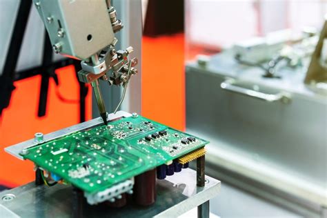
4.2 Manufacturing Considerations
Design for manufacturability is crucial:
- Panelization strategies for small touch sensors
- Solder mask and silkscreen requirements
- Testing access points for production testing
- Tolerance analysis for mechanical fits
4.3 Reliability and Durability
Ensuring long-term operation:
- Conformal coating selection for environmental protection
- Mechanical stress relief for flex connections
- Material selection for thermal cycling resistance
- Vibration-resistant component mounting
Section 5: Advanced Topics in Display PCB Design
5.1 High-Density Interconnect (HDI) Techniques
Meeting demands for higher resolution displays:
- Microvia technology for dense routing
- Fine-pitch component packaging
- Sequential lamination processes
- Embedded component technology
5.2 Flexible and Rigid-Flex PCBs
Growing applications in modern displays:
- Material selection for flexible circuits
- Bend radius considerations
- Transition areas between rigid and flexible sections
- Dynamic flexing vs. static bend applications
5.3 Emerging Technologies
Future directions in display PCB design:
- Mini/Micro-LED display challenges
- Advanced touch technologies (force touch, haptic feedback)
- Integration with wireless communication modules
- Energy harvesting for low-power applications
Conclusion
PCB design for LED and touch screen displays represents a specialized field that blends traditional circuit design principles with unique display-specific requirements. Successful designs must balance electrical performance, thermal management, mechanical constraints, and manufacturing realities. As display technologies continue to advance toward higher resolutions, faster response times, and more sophisticated interactive capabilities, PCB designers must adapt with innovative solutions. By understanding the fundamental principles outlined in this article and staying abreast of emerging technologies, engineers can create robust, high-performance PCBs that form the backbone of modern display systems.
The future of display PCB design will likely see increased integration of functions, continued miniaturization, and the adoption of novel materials and manufacturing techniques. Designers who master both the technical aspects and the system-level thinking required for these complex boards will be well-positioned to meet the growing demands of the display industry.