PCB Design for Manufacturability and Assembly: Key Considerations for Optimal Production
Introduction
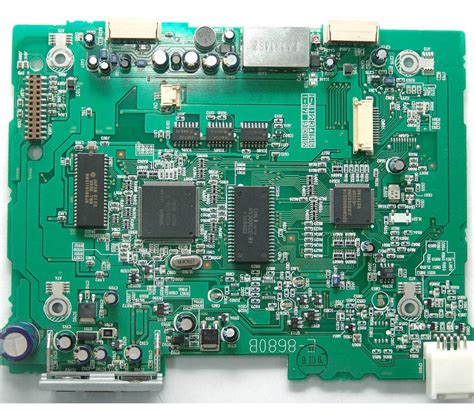
Printed Circuit Board (PCB) design is a critical phase in electronics development, bridging the gap between conceptual schematics and physical hardware. However, even the most innovative circuit designs can face significant challenges during manufacturing and assembly if not properly optimized. Design for Manufacturability (DFM) and Design for Assembly (DFA) are essential methodologies that ensure PCBs are not only functional but also cost-effective and reliable when mass-produced.
This article explores the key principles of PCB design that enhance manufacturability and assembly efficiency. We will discuss common pitfalls, industry best practices, and actionable strategies to improve yield rates, reduce production costs, and minimize defects.
1. Understanding PCB Manufacturability (DFM)
1.1 What is DFM?
DFM refers to designing PCBs in a way that simplifies the fabrication process, minimizes defects, and reduces costs. A manufacturable PCB considers factors such as material selection, trace routing, layer stack-up, and tolerance management.
1.2 Key DFM Considerations
1.2.1 Material Selection
- Substrate Materials: FR-4 is the most common, but high-frequency applications may require Rogers or polyimide.
- Copper Weight: Thicker copper (e.g., 2 oz) improves current handling but complicates etching.
- Surface Finish: HASL, ENIG, and immersion silver impact solderability and cost.
1.2.2 Trace and Space Design
- Minimum Trace Width/Spacing: Follow manufacturer capabilities (e.g., 4/4 mil for standard fab).
- Impedance Control: Critical for high-speed designs; requires precise dielectric management.
1.2.3 Via Design
- Through-Hole vs. Blind/Buried Vias: Complex via structures increase cost.
- Via Size and Pad Diameter: Ensure drill-to-copper ratio is manufacturable.
1.2.4 Panelization and Fiducials
- Panel Design: Use breakaway tabs or V-grooves for efficient assembly.
- Fiducial Marks: Aid pick-and-place machines in component alignment.
2. Design for Assembly (DFA) Considerations
2.1 What is DFA?
DFA focuses on simplifying the assembly process by optimizing component placement, solderability, and mechanical fit. Poor DFA leads to misaligned components, tombstoning, or solder bridges.
2.2 Key DFA Guidelines
2.2.1 Component Placement
- Orientation: Align similar components in the same direction for automated assembly.
- Spacing: Maintain sufficient clearance for reflow soldering and rework.
2.2.2 Footprint and Pad Design
- Land Patterns: Follow IPC-7351 standards to avoid tombstoning or skewed parts.
- Solder Mask Relief: Prevent solder bridging with proper mask definitions.
2.2.3 Thermal Management
- Thermal Pads: Use thermal reliefs for even heat distribution.
- Heat-Sensitive Components: Keep them away from high-power devices.
2.2.4 Testability and Rework
- Test Points: Include accessible test pads for in-circuit testing (ICT).
- Rework Access: Ensure enough space for soldering irons or hot air guns.
3. Common DFM/DFA Pitfalls and How to Avoid Them
3.1 Insufficient Design Rule Checks (DRC)
- Problem: Ignoring manufacturer-specific DRCs leads to rejected boards.
- Solution: Use automated DRC tools and consult fabrication notes.
3.2 Poor Layer Stack-Up Planning
- Problem: Incorrect impedance or signal integrity issues.
- Solution: Simulate stack-ups and validate with the manufacturer.
3.3 Overlooking Solder Paste Stencil Design
- Problem: Inconsistent solder deposition causes weak joints.
- Solution: Optimize stencil aperture ratios (e.g., 1:1 for standard components).
3.4 Ignoring Assembly Tolerances
- Problem: Misaligned components due to placement inaccuracies.
- Solution: Account for pick-and-place machine tolerances (±0.05 mm typical).
4. Tools and Techniques for DFM/DFA Optimization
4.1 Software Tools
- Cadence Allegro, Altium Designer, and KiCad offer built-in DFM checks.
- Valor NPI and CAM350 provide advanced fabrication analysis.
4.2 Prototyping and Testing
- Order Prototypes: Test manufacturability before full production.
- Assembly Trials: Validate pick-and-place performance.
4.3 Collaboration with Manufacturers
- Early Engagement: Involve fabricators during the design phase.
- Feedback Loops: Incorporate their DFM/DFA suggestions.
5. Conclusion
Designing PCBs with manufacturability and assembly in mind is not optional—it’s a necessity for reducing costs, improving yield, and ensuring reliability. By adhering to DFM/DFA principles, engineers can avoid costly redesigns, delays, and field failures.
Key Takeaways:
✅ DFM ensures fabrication feasibility (trace width, material selection, via design).
✅ DFA optimizes assembly efficiency (component placement, solderability, testability).
✅ Use automated tools and manufacturer feedback to refine designs.
✅ Prototype early to catch issues before mass production.
By integrating these best practices, PCB designers can achieve a seamless transition from design to production, delivering high-quality boards that meet both performance and manufacturability requirements.