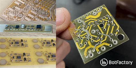
PCB Design for Manufacturability (DFM)
DFM: Design for Manufacture
DFM means design for manufacturing, Design for manufacturability, that is, starting from improving the manufacturability of parts, making parts and various processes easy to manufacture, low manufacturing cost, high efficiency, and low cost ratio.
It is to fully consider the difficulties that may be encountered in the production link during the design stage, and to design in order to reduce production problems, improve production efficiency, and reduce production costs. This includes hardware design and software design.

1.DFM analysis stage
DFM analysis at different stages can achieve different results. It is better to find problems at an early stage. The worst thing is that some companies cannot recognize that this is a DFM problem.
The earlier the DFM stage, the easier it is to solve the problems found, and the smaller the loss.
DFM does not simply refer to production itself, but is also related to the following other DFx:
2.DFM process requirements for PCB design
(1)Size range
The external dimensions must not exceed the processing capacity of the equipment
The commonly used size range is “width (200 mm ~ 250 mm) × length (250 mm ~ 350 mm)”. For PCBs with a long side size less than 125 mm or a short side less than 100 mm, or irregular shaped edges, they need to be designed as panels.
(2)External shape
The external shape of the board is rectangular. If panelization is not required, the four corners of the board are required to be rounded; if panelization is required, the four corners of the board after panelization are required to be rounded, and the minimum radius of the rounded corner is r = 1mm, and r = 2.0mm is recommended.
In order to ensure the stability of the transmission process, the design should consider using the process panelization method to convert irregular shaped PCBs into rectangular shapes, especially the corner gaps should be filled.
For pure SMT boards, gaps are allowed, but the size of the gap must be less than 1/3 of the length of the edge to ensure that the PCB is smoothly transported on the chain.
For the inner fillet, the recommended minimum radius is 0.8mm. If necessary, the radius can be as small as 0.4mm.
For the design requirements of the gold finger, see the figure. In addition to the chamfering of the insertion edge as required, the sides of the plug-in board
should also be designed with (1~1.5)×45° chamfers or R1~R1.5 fillets.
(3)Transfer edge
In order to reduce the deformation of the PCB during welding, for PCBs without paneling, the long side direction is generally used as the transfer direction; for paneling, the long side direction should also be used as the transfer direction. For PCBs with a ratio of short side to long side greater than 80%, the short side can be used for transfer.
Since the terminal single board generally adopts paneling design, the process edge is generally used as the transmission edge, and the narrowest width of the process edge is generally not less than 4.5mm.
(4)MARK point
Optical positioning reference symbol (also known as MARK point)
Mark point, also called reference point, provides a common measurable point for all steps in the assembly process, ensuring that each device used in the assembly can accurately locate the circuit pattern. Therefore, the mark point is crucial to SMT production.
Mark point is the position identification point of the PCB used on the automatic placement machine in the circuit board design. The selection of mark point directly affects the placement efficiency of the automatic placement machine.
Generally, the selection of mark point is related to the model of the automatic placement machine.
4.MARK point
Optical positioning reference symbol (also known as MARK point)
Mark point, also called reference point, provides a common measurable point for all steps in the assembly process, ensuring that each device used in the assembly can accurately locate the circuit pattern. Therefore, the mark point is crucial to SMT production.
Mark point is the position identification point of the PCB used on the automatic placement machine in the circuit board design. The selection of mark point directly affects the placement efficiency of the automatic placement machine.
Generally, the selection of mark point is related to the model of the automatic placement machine.
MARK point shape: The preferred shape of the mark point is a solid circle with a diameter of 1mm (±0.2mm), and the material is bare copper (which can be protected by a clear anti-oxidation coating), tin plating or nickel plating. Attention should be paid to flatness, smooth and neat edges, and the color should be clearly different from the surrounding background color.
In order to ensure the recognition effect of printing equipment and placement equipment, there should be no other routing, silk screen, pads or wait-cut in the empty area of the MARK point.
The mark point is required to be marked as a solid circle; a complete mark point includes: a mark point (or feature point) and an open area.
1) The relative diagonal positions of the mark points on the circuit board or the combined board should be as far apart as possible, preferably distributed at the longest diagonal position;
2) To ensure the requirements of mounting accuracy, SMT equipment requires: In all products produced by SMT, each PCB board must have at least one pair of mark points that meet the design requirements and can be recognized by the SMT machine. Single board mark can be considered (for single board and panel, the position of the mark in the board is shown in the figure below). Panel mark or combined mark only serves as an auxiliary positioning function.
3) When panelizing, the relative position of the mark points of each single board must be the same. The position of the MARK point on any single board in the panel cannot be moved for any reason, which will cause the position of the MARK points of each single board to be asymmetric.
Special panelization method:
① The diagonal MARK position must be the same for the yin-yang board
② The MARK positions of the mirror board must be the same. R1=R2
4) All MARK points on the PCB board are only valid if they meet the following conditions: two MARKs on the same diagonal line and appear in pairs. Therefore, the MARK points must appear in pairs to be used.
Size:
1) The minimum diameter of the Mark point mark is 1.0mm and the maximum diameter is 3.0mm. The size variation of the mark on the same printed circuit board cannot exceed 25 microns;
2) Special emphasis: the size of all mark points on the same board number PCB must be consistent (including PCBs of the same board number produced by different manufacturers)
3) It is recommended that RD-layout unify the diameter of the mark points of all drawings to 1.0mm;
Edge distance:
1) The distance between the mark point (edge) and the edge of the printed circuit board must be ≥5.0mm (the minimum spacing requirement for the machine clamp PCB), and must be inside the PCB board rather than on the edge of the board, and meet the minimum mark point openness requirement. Emphasis: It refers to the distance between the edge of the MARK point and the edge of the board ≥3.0mm, not the center of the MARK point.
Openness requirement: There must be an open area around the mark point without other circuit features or marks. The radius of the open area circle r≥2R, R is the radius of the MARK point, and when r reaches 3R, the machine recognition effect is better. Increase the color contrast between the MARK point and the environment. No characters (copper cladding or silk screen, etc.) are allowed in r
Material: Marks can be bare copper, bare copper protected by a clear anti-oxidation coating, nickel or tin plating, or
solder coating. If solder mask is used, it should not cover the mark point or its open area. Flatness: The surface flatness of the mark point should be within 15 microns [0.0006″]. Contrast: a) The best performance can be achieved when there is a high contrast between the mark point and the substrate material of the printed board. b) The inner layer background of all mark points must be the same.
5. Positioning holes.
Each PCB should be designed with at least two positioning holes at its corners. There should be four positioning holes in the panel, distributed at the four corners, and the standard aperture of the positioning holes is 2.00±0.08mm. The center distance of the positioning holes is close to the board edge is 5mm. The minimum distance between the device or pad next to the positioning hole and the edge of the positioning hole should be at least 1.5mm.
6. Hole metallization problem.
Positioning holes and non-grounded mounting holes should generally be designed as non-metallized holes.