PCB Design Guide for Decoupling Capacitor Placement
Introduction
Decoupling capacitors are essential components in printed circuit board (PCB) design, serving to stabilize power supply voltages and reduce noise in high-speed digital and analog circuits. Proper placement and selection of decoupling capacitors can significantly impact signal integrity, power delivery network (PDN) performance, and electromagnetic compatibility (EMC).
This guide provides best practices for placing decoupling capacitors in PCB designs, covering key considerations such as capacitor selection, placement strategies, and layout techniques to optimize performance.
1. The Role of Decoupling Capacitors
Decoupling capacitors serve two primary functions:
- Bypassing High-Frequency Noise – They provide a low-impedance path for high-frequency noise to ground, preventing it from propagating through the power distribution network.
- Local Energy Storage – They supply instantaneous current to ICs during transient switching events, reducing voltage fluctuations.
Without proper decoupling, power supply noise can lead to signal integrity issues, increased electromagnetic interference (EMI), and even circuit malfunction.
2. Types of Decoupling Capacitors
Different capacitor types are used depending on frequency requirements:
- Bulk Capacitors (10µF – 100µF) – Used for low-frequency stabilization, typically placed near voltage regulators.
- Ceramic Capacitors (0.1µF – 1µF) – Most common for mid-frequency decoupling (1MHz – 100MHz).
- Small-Value Capacitors (1nF – 100nF) – Used for high-frequency noise suppression (>100MHz).
A combination of capacitors is often necessary to cover a wide frequency range.
3. Key Placement Guidelines
3.1 Proximity to Power Pins
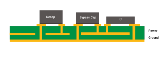
The most critical rule in decoupling capacitor placement is minimizing the loop inductance between the capacitor and the IC power pins. Follow these best practices:
- Place capacitors as close as possible to the power and ground pins of the IC.
- Use short and wide traces to reduce parasitic inductance.
- Avoid vias between the capacitor and the IC if possible, as they introduce additional inductance.
3.2 Multiple Capacitors for Different Frequencies
A single capacitor cannot effectively suppress noise across all frequencies. Instead, use:
- A large bulk capacitor (e.g., 10µF) near the voltage regulator.
- Medium-value capacitors (e.g., 0.1µF) near each IC power pin.
- Small-value capacitors (e.g., 1nF – 10nF) for high-frequency noise suppression.
3.3 Power and Ground Plane Considerations
- Use solid ground planes to provide a low-impedance return path.
- Place capacitors between the power and ground planes to enhance decoupling effectiveness.
- Avoid splitting ground planes under decoupling capacitors, as this increases loop inductance.
3.4 Via Placement and Routing
- If vias are necessary, use multiple vias in parallel to reduce inductance.
- Route capacitor connections symmetrically to minimize loop area.
- Avoid daisy-chaining capacitors; instead, connect each directly to the power and ground planes.
3.5 High-Speed and RF Designs
For high-frequency circuits (e.g., RF, DDR memory, processors):
- Use multiple small capacitors (e.g., 0.01µF – 0.1µF) in parallel.
- Place capacitors on both sides of the PCB (if space permits) to reduce loop inductance.
- Consider embedded capacitance in advanced designs for ultra-high-frequency decoupling.
4. Common Mistakes to Avoid
4.1 Incorrect Capacitor Selection
- Using only one large capacitor instead of a combination for different frequencies.
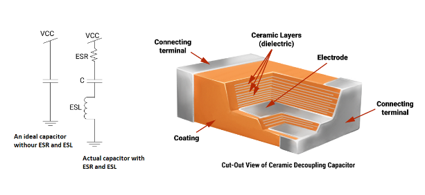
- Choosing capacitors with insufficient voltage ratings or high equivalent series resistance (ESR).
4.2 Poor Placement
- Placing capacitors too far from IC power pins, increasing loop inductance.
- Using long, thin traces instead of short, wide connections.
4.3 Improper Grounding
- Splitting ground planes under decoupling capacitors.
- Not providing a low-impedance return path for high-frequency currents.
4.4 Neglecting High-Frequency Effects
- Ignoring the self-resonant frequency (SRF) of capacitors, leading to ineffective decoupling at certain frequencies.
- Not accounting for parasitic inductance in capacitor leads and traces.

5. Simulation and Verification
To ensure optimal decoupling performance:
- Use PDN (Power Delivery Network) analysis tools (e.g., Ansys SIwave, Cadence Sigrity) to simulate impedance and noise.
- Perform time-domain and frequency-domain analysis to verify decoupling effectiveness.
- Measure power supply noise with an oscilloscope to validate real-world performance.
6. Conclusion
Proper decoupling capacitor placement is crucial for stable power delivery and noise suppression in PCB designs. By following these guidelines—minimizing loop inductance, using multiple capacitor values, and optimizing placement—engineers can significantly improve signal integrity and reduce EMI.
For high-speed designs, additional considerations such as via optimization, ground plane integrity, and advanced simulation techniques are necessary. Always verify decoupling performance through simulation and testing to ensure reliable operation.
By adhering to these best practices, PCB designers can achieve robust, noise-free power distribution, enhancing the overall performance and reliability of electronic systems.