PCB design, how engineers can avoid inferior skills
Many people like design. When designing, people must first master the most basic design skills, and then practice and study continuously. For friends who are determined to be engineers, drawing boards are hard skills. If you don’t practice, you will not succeed. Even if you can remember all the characteristic curves of MOS tubes, you will not be inferior after all. Today, I will share with you how engineers can avoid inferior skills in PCB design!
The basic design process of general PCB is as follows:
Preliminary preparation-PCB structure design-PCB layout-wiring-wiring optimization and silk screen-network and DRC inspection and structure inspection-plate making.
1.Preliminary preparation includes preparing component library and schematic diagram
“If you want to do your work well, you must first sharpen your tools.” To make a good board, in addition to designing the principle, you must also draw well. Before designing PCB, you must first prepare the component library of the schematic diagram SCH and the component library of PCB. The component library can use the library provided by peotel, but it is generally difficult to find a suitable one. It is best to make your own component library based on the standard size information of the selected device. In principle, make the component library of PCB first, and then make the component library of SCH.
The requirements of PCB component library are relatively high, which directly affects the installation of the board; the requirements of SCH component library are relatively loose, as long as you pay attention to defining the pin attributes and the corresponding relationship with PCB components. PS: Pay attention to the hidden pins in the standard library. After that, it is the design of the schematic diagram. After that, you are ready to start PCB design.
2. PCB structure design
In this step, according to the determined circuit board size and various mechanical positioning, draw the PCB board surface in the PCB design environment, and place the required connectors, buttons/switches, screw holes, assembly holes, etc. according to the positioning requirements. And fully consider and determine the wiring area and non-wiring area (such as how much area around the screw hole belongs to the non-wiring area).
3.PCB layout
To put it bluntly, layout is to place devices on the board. At this time, if the preparations mentioned above are done, you can generate a network table on the schematic diagram (Design-》Create Netlist), and then import the network table on the PCB diagram (Design-》Load Nets). You can see all the components stacked up, with flying wires between the pins to indicate the connections. Then you can lay out the components. The general layout is carried out according to the following principles:
1 Reasonable division according to electrical performance, generally divided into: digital circuit area (i.e. afraid of interference and generating interference), analog circuit area (afraid of interference), power drive area (interference source);
2 Circuits that complete the same function should be placed as close as possible, and the components should be adjusted to ensure the simplest connection; at the same time, the relative positions between the functional blocks should be adjusted to make the connection between the functional blocks as simple as possible;
3 For components with large mass, the installation position and installation strength should be considered;
heating components should be placed separately from temperature-sensitive components, and thermal convection measures should be considered if necessary;
4 I/O driver devices should be as close to the edge of the printed board and the lead-out connector as possible;
5 Clock generators (such as crystal oscillators or clock oscillators) should be as close as possible to the devices that use the clock;
6 A decoupling capacitor (generally a monolithic capacitor with good high-frequency performance) should be added between the power input pin and the ground of each integrated circuit; when the circuit board space is dense, a tantalum capacitor can also be added around several integrated circuits.
7.Add a discharge diode (1N4148 is enough) to the relay coil;
8.The layout should be balanced, orderly and dense, and should not be top-heavy or heavy on one side.
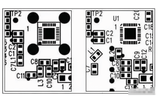
Special attention should be paid to the placement of components. The actual size (area and height) and relative position of components should be considered to ensure the electrical performance of the circuit board and the feasibility and convenience of production and installation. At the same time, the placement of components should be appropriately modified to make them neat and beautiful, while ensuring that the above principles can be reflected. For example, the same components should be placed neatly and in the same direction, and should not be placed “staggered”.
This step is related to the overall image of the board and the difficulty of the next wiring, so it is necessary to spend a lot of effort to consider it. When laying out, preliminary wiring can be done for places that are not sure, and full consideration should be given.
14.wiring
Wiring is the most important process in the entire PCB design. This will directly affect the performance of the PCB board. In the design process of PCB, wiring is generally divided into three levels: the first is wiring, which is the most basic requirement for PCB design. If the circuits are not connected and there are flying wires everywhere, it will be an unqualified board, which can be said to be not yet started. The second is the satisfaction of electrical performance.
This is the standard for measuring whether a printed circuit board is qualified.
This is after the wiring is connected, carefully adjust the wiring to achieve the best electrical performance. Next is the appearance. If your wiring is connected, there is nothing that affects the electrical performance, but it looks messy at first glance, plus colorful and colorful, then no matter how good your electrical performance is, it is still a piece of garbage in the eyes of others. This brings great inconvenience to testing and maintenance. The wiring should be neat and uniform, and it cannot be criss-crossed and disorderly. These must be achieved while ensuring the performance of the electrical appliances and meeting other individual requirements, otherwise it will be a waste of effort.
Five main principles for wiring
Generally, the power line and ground line should be wired first to ensure the electrical performance of the circuit board. As far as conditions allow, try to widen the width of the power and ground wires. It is best that the ground wire is wider than the power wire. The relationship between them is: ground wire>power wire>signal wire. Usually the signal wire width is: 0.2~0.3mm, the thinnest width can reach 0.05~0.07mm, and the power wire is generally 1.2~2.5mm. For the PCB of digital circuits, a wide ground wire can be used to form a loop, that is, to form a ground network for use (the ground of analog circuits cannot be used in this way).
- Pre-wire the wires with stricter requirements (such as high-frequency wires). The edge wires of the input and output ends should avoid adjacent parallel to avoid reflection interference. If necessary, ground wire isolation should be added. The wiring of two adjacent layers should be perpendicular to each other. Parallel is prone to parasitic coupling.
- The oscillator shell is grounded, and the clock line should be as short as possible and cannot be led everywhere. Under the clock oscillator circuit and the special high-speed logic circuit, the ground area should be increased, and other signal lines should not be used to make the surrounding electric field approach zero;
- Use 45o folded line wiring as much as possible, and do not use 90o folded line to reduce the radiation of high-frequency signals; (high-requirement lines should also use double arc lines)
- No signal line should form a loop. If it is unavoidable, the loop should be as small as possible; the vias of the signal line should be as few as possible;
- The key line should be as short and thick as possible, and add protective ground on both sides.
- When transmitting sensitive signals and noise field band signals through flat cables, use the “ground wire-signal-ground wire” method to lead them out.
- Test points should be reserved for key signals to facilitate production and maintenance inspection. After the schematic wiring is completed, the wiring should be optimized;
- At the same time, after the initial network inspection and DRC inspection are correct, fill the unwired area with ground wires, use a large area of copper layer as the ground wire, and connect the unused areas on the printed circuit board to the ground as the ground wire. Or make a multi-layer board, with the power supply and ground wire occupying one layer each


