PCB Design & Manufacturing Best Practices for Error Reduction

Key Takeaways
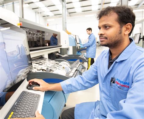
Understanding PCB manufacturing fundamentals helps you avoid costly mistakes from the design phase onward. When working with PCB manufacturing companies, prioritize design for manufacturability (DFM) principles to align your layouts with fabrication capabilities. For instance, adhering to minimum trace spacing and drill hole tolerances reduces rework risks, directly lowering PCB manufacturing cost.
"Always validate your design files with your manufacturer’s guidelines before finalizing—this simple step can save weeks of delays."
Optimizing panelization techniques not only streamlines production but also maximizes material usage, a critical factor for scaling your PCB manufacturing business. Use automated DFM checkers to flag issues like copper imbalances or insufficient solder mask clearance, which are common culprits for assembly errors. For deeper insights, explore industry-leading DFM strategies to refine your approach. By integrating these practices early, you ensure smoother transitions from prototyping to mass production while maintaining quality consistency.

DFM Fundamentals for PCB Design Success
To achieve success in PCB manufacturing, mastering design for manufacturability (DFM) principles is non-negotiable. By aligning your design choices with the capabilities of PCB manufacturing companies, you minimize risks of fabrication errors and delays. Start by understanding your manufacturer’s technical guidelines—common requirements include minimum trace widths, spacing tolerances, and drill hole sizes. Ignoring these standards often escalates PCB manufacturing cost due to rework or specialized tooling.
For example, placing components too close to board edges might violate assembly machine limits, forcing your PCB manufacturing business partner to manually adjust placements. Use design software with built-in DFM checks to flag such issues early. Below is a comparison of critical DFM parameters for cost optimization:
| Design Aspect | Non-DFM Approach | DFM-Optimized Approach |
|---|---|---|
| Trace Spacing | 4 mil | 6 mil (standard) |
| Via Size | 8 mil drill | 10 mil drill |
| Component Placement | Edge proximity <1mm | Edge proximity >2mm |
| Cost Impact | High rework fees | Lower per-unit cost |
Prioritize collaboration with your manufacturer during prototyping. Clarify material preferences, layer stack-up tolerances, and testing protocols to ensure alignment. By embedding DFM thinking early, you reduce time-to-market while improving reliability—key factors in sustaining competitiveness in PCB manufacturing.
Optimizing Layouts for Manufacturing Efficiency
When designing circuit boards, how you arrange components directly impacts pcb manufacturing efficiency and cost-effectiveness. Start by aligning your layout with design for manufacturing (DFM) principles: maintain consistent trace widths, avoid acute angles in routing, and ensure adequate spacing between high-voltage components. These choices minimize production complexities, reducing the risk of errors during fabrication.
Collaborating early with pcb manufacturing companies helps identify potential bottlenecks. For instance, grouping surface-mount devices (SMDs) on one side of the board simplifies assembly workflows, lowering pcb manufacturing cost by minimizing machine recalibration. Use standardized drill sizes and panelization strategies to optimize material usage—this not only cuts waste but also improves throughput for high-volume orders.
Pay attention to copper balancing and thermal relief patterns. Uneven copper distribution can warp boards during soldering, escalating rework costs in the pcb manufacturing business. Tools like automated design rule checks (DRC) verify compliance with fabrication tolerances, ensuring your design aligns with industry-standard IPC-2221 guidelines. By prioritizing manufacturability in layout planning, you create boards that transition seamlessly from prototype to mass production while maintaining quality.
Key Fabrication Standards for Error-Free PCBs
Adhering to industry-recognized fabrication standards ensures your PCB manufacturing process minimizes defects while maintaining efficiency. Start by validating design files against IPC-6012 and IPC-A-600 specifications, which define acceptable criteria for material quality, hole wall integrity, and surface finishes. Reputable PCB manufacturing companies prioritize these benchmarks to avoid common pitfalls like copper thinning or delamination.
When optimizing PCB manufacturing cost, balance material choices with performance requirements. For instance, specifying FR-4 substrates for standard applications reduces expenses compared to high-frequency laminates, while still meeting thermal and electrical needs. Always confirm trace/spacing tolerances with your fabrication partner—designs exceeding a manufacturer’s minimum feature capabilities risk costly reworks.
Implementing DFM (Design for Manufacturing) checks early—such as verifying annular ring widths or solder mask clearances—helps align your design with production realities. This proactive approach not only streamlines the PCB manufacturing business workflow but also prevents assembly-stage errors. Finally, insist on automated optical inspection (AOI) and electrical testing protocols to catch deviations before boards leave the facility. By integrating these standards, you create a foundation for reliability across high-volume or complex projects.
Assembly Error Prevention Through Smart Design
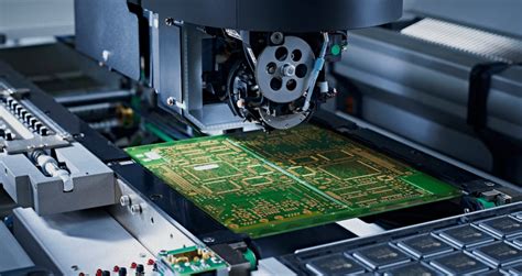
Smart design decisions directly influence assembly success rates in PCB manufacturing. Start by optimizing component placement to minimize cross-interference and ensure adequate spacing for automated pick-and-place systems. Over 60% of assembly errors stem from mismatched footprints, so always verify land pattern accuracy against your chosen PCB manufacturing companies’ capabilities. Implement symmetrical pad designs for surface-mount devices (SMDs) to prevent tombstoning, and use fiducial markers aligned with IPC-7351 standards to enhance machine vision accuracy.
When designing for high-density interconnects (HDIs), prioritize thermal relief patterns to avoid solder wicking during reflow processes. Collaborate early with your PCB manufacturing business partner to validate stack-up configurations and material choices—this reduces impedance mismatches that often lead to rework. For cost-sensitive projects, balance PCB manufacturing cost considerations by standardizing hole sizes and avoiding non-standard via geometries, which complicate drilling and plating.
Leverage automated DFM (Design for Manufacturability) checks to flag potential short circuits or insufficient solder mask clearances. Incorporate test points for in-circuit testing (ICT) and boundary scan access, ensuring your design aligns with the PCB manufacturing facility’s quality protocols. By integrating these strategies, you’ll mitigate risks like misplaced components or cold joints while maintaining scalability for volume production.

Cost-Effective Manufacturing Techniques Revealed
To minimize PCB manufacturing cost without compromising quality, you need to adopt strategies that streamline production while maintaining reliability. Start by standardizing design elements like pad sizes and trace widths, which reduce variability during fabrication. Partnering with experienced PCB manufacturing companies that offer design-for-manufacturability (DFM) feedback ensures your layouts align with their equipment’s capabilities, avoiding costly redesigns.
Another key strategy is optimizing panelization. Arranging multiple boards on a single panel maximizes material usage and reduces waste—a critical factor for scaling your PCB manufacturing business. For high-volume orders, negotiate bulk pricing for materials like FR-4 substrates or specialty laminates, as suppliers often offer discounts for larger quantities.
Proactive communication with your manufacturer about tolerances and testing requirements also prevents over-engineering. For instance, specifying tighter tolerances only where electrically necessary lowers PCB manufacturing cost by simplifying processes. Additionally, leveraging automated optical inspection (AOI) and flying probe testing early in production identifies defects before assembly, reducing rework expenses.
Finally, consider hybrid manufacturing approaches. Combining traditional subtractive methods with additive techniques for complex layers can cut material costs by up to 20%. By focusing on these cost-driven optimizations, you ensure your designs meet both performance goals and budgetary constraints.
Material Selection Impact on PCB Reliability
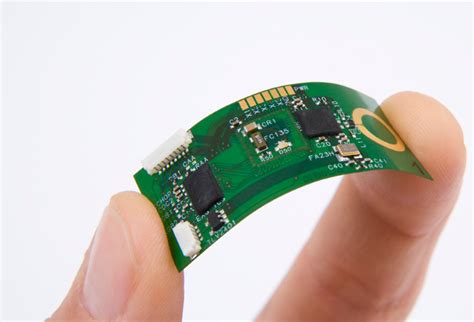
Choosing the right materials directly influences your PCB’s long-term performance and durability. Substrate selection, for instance, determines thermal stability and mechanical resilience. Opt for PCB manufacturing-grade laminates like FR-4 for standard applications, but consider high-Tg (glass transition temperature) materials or polyimide for environments with extreme heat or vibration. These choices prevent warping, delamination, and signal loss—common failures that escalate PCB manufacturing cost due to rework or replacements.
Copper weight and dielectric properties also play pivotal roles. Thicker copper traces improve current handling but require precise etching to avoid over- or under-etching during fabrication. Partnering with experienced PCB manufacturing companies ensures material compatibility with their processes, reducing risks of impedance mismatches or layer misalignment. For high-frequency designs, low-Dk (dielectric constant) materials minimize signal distortion, though they may increase PCB manufacturing business expenses.
Balancing performance and budget means evaluating thermal conductivity and coefficient of thermal expansion (CTE). Mismatched CTE between layers can cause cracks during thermal cycling. By aligning material properties with operational demands, you mitigate reliability risks while optimizing PCB manufacturing workflows. This becomes critical when scaling production, where even minor material flaws can compound into systemic failures.
Thermal Management Strategies in Circuit Design
Effective thermal management begins with understanding how heat flows through your PCB manufacturing process. Poor thermal design not only risks component failure but also increases PCB manufacturing cost due to rework or premature replacements. Start by optimizing copper distribution: thicker traces or planes in high-current areas reduce resistance and heat buildup. Use thermal vias beneath power-hungry components like ICs or voltage regulators to channel heat away from critical layers, a technique widely adopted by leading PCB manufacturing companies.
When working with PCB manufacturing business partners, verify their capabilities in handling advanced materials like metal-core substrates or high-Tg laminates for applications requiring superior heat dissipation. Implement thermal relief pads in through-hole components to minimize soldering defects while maintaining efficient heat transfer. Simulation tools like finite element analysis (FEA) can predict hotspots during design, allowing you to adjust layouts before production—saving time and aligning with fabrication standards for reliability.
Finally, balance airflow considerations with component placement. Dense layouts might require strategic spacing or angled orientations to enhance convection cooling. By integrating these practices early, you ensure designs meet both performance goals and the economic realities of PCB manufacturing, reducing long-term operational risks.

Quality Control Protocols for Precision PCBs
Implementing rigorous quality control protocols ensures your precision PCB designs transition seamlessly into reliable physical products. Leading PCB manufacturing companies deploy multi-stage inspection systems, starting with automated optical inspection (AOI) to detect soldering defects or trace misalignments. For high-density boards, X-ray imaging verifies internal layer integrity, while in-circuit testing (ICT) validates electrical performance against design specifications.
To optimize PCB manufacturing cost without compromising quality, establish clear acceptance criteria with your fabrication partner early. This includes defining tolerance thresholds for trace widths, hole diameters, and solder mask alignment. Statistical process control (SPC) tools track variations across production batches, allowing proactive adjustments before errors escalate.
In the PCB manufacturing business, documentation proves critical. Maintain detailed records of material certifications, surface finish specifications, and thermal cycling test results. For mission-critical applications, consider adding burn-in testing to simulate operational stresses. By aligning these protocols with your design intent, you reduce rework cycles and strengthen partnerships with manufacturers focused on delivering error-free boards.
Conclusion
By implementing robust DFM strategies throughout your design phase, you position PCB manufacturing projects for success from concept to delivery. Partnering with experienced PCB manufacturing companies ensures your designs align with their production capabilities, reducing costly revisions. To optimize PCB manufacturing cost, prioritize standardized materials and modular layouts that simplify assembly while maintaining reliability—critical factors for scaling any PCB manufacturing business.
When selecting components, consider how thermal profiles and tolerance thresholds affect both performance and long-term maintenance expenses. Proactive communication with fabricators about stack-up configurations and finish requirements prevents mismatches that escalate PCB manufacturing cost. Remember that design choices impacting PCB manufacturing efficiency—like panelization methods or solder mask clearances—directly influence yield rates and defect probabilities.
Ultimately, reducing errors requires viewing design and fabrication as interconnected stages. By validating layouts against IPC standards early and conducting DFM audits with your manufacturer, you create a feedback loop that strengthens process control. As you refine these practices, track metrics like first-pass yield and scrap rates to quantify improvements—evidence-based insights that drive competitiveness in the PCB manufacturing business landscape.

FAQs
How does PCB manufacturing affect final product reliability?
Working with certified PCB manufacturing companies ensures adherence to IPC-6012 standards, which govern material quality and fabrication tolerances. Properly vetted partners minimize risks of delamination or electrical failures in high-stress environments.
What factors influence PCB manufacturing cost?
Key variables include board complexity, layer count, and material selection. High-density interconnect (HDI) designs often raise costs, but collaborating with experienced PCB manufacturing business partners can optimize panel utilization and reduce waste through design-for-manufacturability (DFM) reviews.
How can design choices lower assembly errors?
Implementing solder mask-defined pads and avoiding component shadowing during layout reduces soldering defects. Most PCB manufacturing providers offer automated optical inspection (AOI) feedback to refine designs before mass production.
When should you engage PCB manufacturing companies in the design phase?
Early consultation prevents non-recurring engineering (NRE) charges from late-stage revisions. Reputable firms provide thermal simulation insights and impedance control guidance to align your design with their process capabilities.
Ready to Optimize Your PCB Project?
For tailored PCB manufacturing solutions that balance quality and PCB manufacturing cost, please click here to connect with industry experts.