PCB Design Methods for Noise Suppression
Abstract
Noise suppression is a critical aspect of printed circuit board (PCB) design, affecting signal integrity, electromagnetic compatibility (EMC), and overall system performance. This paper explores various techniques to minimize noise in PCB designs, including proper grounding, shielding, trace routing, decoupling, and component placement. By implementing these methods, designers can reduce electromagnetic interference (EMI), crosstalk, and power supply noise, ensuring reliable operation in high-frequency and mixed-signal applications.
1. Introduction
With the increasing complexity and speed of modern electronic circuits, noise suppression has become a major challenge in PCB design. Noise can originate from multiple sources, such as switching signals, power supply fluctuations, and external electromagnetic interference. If not properly managed, noise can degrade signal quality, cause data corruption, and even lead to system failures. This paper discusses key PCB design strategies to mitigate noise and improve circuit performance.
2. Sources of Noise in PCBs
Understanding the sources of noise is essential for effective suppression. Common noise sources include:
- Conducted Noise: Propagates through power and ground traces.
- Radiated Noise: Generated by high-frequency signals and electromagnetic fields.
- Crosstalk: Unwanted coupling between adjacent traces.
- Ground Bounce: Voltage fluctuations in ground planes due to high-speed switching.
- Power Supply Noise: Ripple and transient disturbances in power lines.
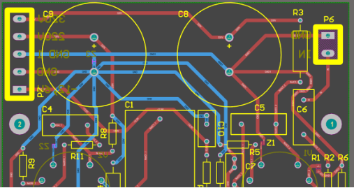
3. PCB Design Techniques for Noise Suppression
3.1 Proper Grounding Techniques
A well-designed grounding system is fundamental to noise reduction. Key methods include:
- Single-Point Grounding: Suitable for low-frequency circuits to avoid ground loops.
- Multi-Point Grounding: Used in high-frequency designs to minimize impedance.
- Ground Plane: A continuous copper plane reduces ground impedance and provides a low-inductance return path.
- Split Ground Planes: Separating analog and digital grounds to prevent noise coupling, with a single connection point.
3.2 Power Supply Decoupling
Decoupling capacitors stabilize power supply voltages and filter high-frequency noise. Best practices include:
- Placement: Locate decoupling capacitors as close as possible to IC power pins.
- Multiple Capacitor Values: Use a combination of bulk (10µF), ceramic (0.1µF), and high-frequency (1nF) capacitors to cover a wide frequency range.
- Low-ESR Capacitors: Reduce equivalent series resistance for better high-frequency performance.
3.3 Signal Routing Strategies
Proper trace routing minimizes crosstalk and EMI:
- Controlled Impedance Traces: Match trace impedance to the source and load to prevent reflections.
- Minimize Parallel Trace Lengths: Reduce capacitive and inductive coupling between signals.
- Differential Pair Routing: Use tightly coupled differential pairs for high-speed signals to reject common-mode noise.
- Avoid Sharp Bends: Use 45° or curved traces to reduce impedance discontinuities.
3.4 Shielding and EMI Reduction
Shielding techniques help contain electromagnetic emissions:
- Faraday Cages: Enclose sensitive circuits in conductive enclosures.
- Guard Traces: Place grounded traces next to sensitive signals to block interference.
- Via Fencing: Use rows of grounded vias around high-frequency traces to reduce radiation.
3.5 Component Placement and Layout
Optimal component placement reduces noise coupling:
- Partitioning: Separate analog, digital, and RF sections to minimize interference.
- Short Signal Paths: Reduce trace lengths for high-speed signals to lower inductance.
- Orientation: Place components to minimize loop areas and cross-coupling.
3.6 Filtering Techniques
Filters attenuate unwanted noise frequencies:
- Ferrite Beads: Block high-frequency noise on power and signal lines.
- LC Filters: Used for power supply noise suppression.
- RC Filters: Reduce high-frequency noise in signal paths.
4. Simulation and Testing for Noise Analysis
Before fabrication, noise analysis tools can predict and mitigate issues:
- SPICE Simulations: Analyze power integrity and signal behavior.
- EMI/EMC Simulation Tools: Identify radiation hotspots.
- Time-Domain Reflectometry (TDR): Detect impedance mismatches.
- Spectrum Analyzers: Measure conducted and radiated emissions.
5. Case Study: Noise Reduction in a Mixed-Signal PCB
A case study demonstrates how applying these techniques improved noise performance in a mixed-signal ADC/DAC system:
- Problem: Excessive noise coupling between analog and digital sections.
- Solution: Implemented split ground planes, optimized decoupling, and used guard traces.
- Result: Reduced noise by 15dB and improved signal-to-noise ratio (SNR).
6. Conclusion
Effective noise suppression in PCB design requires a combination of proper grounding, decoupling, routing, shielding, and filtering techniques. By carefully analyzing noise sources and applying best practices, designers can enhance signal integrity, reduce EMI, and ensure reliable circuit operation. Future advancements in materials and simulation tools will further improve noise management in high-speed and RF applications.


