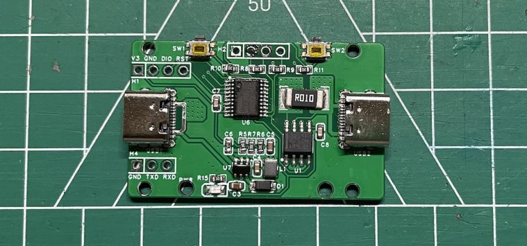
PCB Design Practical Tips: Essential Techniques for Success
Printed Circuit Board (PCB) design is a critical aspect of electronic product development. Whether you’re a beginner or an experienced engineer, mastering practical PCB design techniques can significantly improve performance, reliability, and manufacturability. This article explores key PCB design tips, covering layout, routing, signal integrity, power distribution, and manufacturing considerations.
1. Smart Component Placement
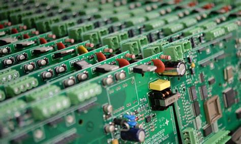
Proper component placement is the foundation of a well-designed PCB. Poor placement can lead to signal integrity issues, thermal problems, and manufacturing difficulties.
Key Tips:
- Group Related Components: Place components that interact closely (e.g., microcontroller and its peripherals) near each other to minimize trace lengths.
- Consider Signal Flow: Arrange components to follow the natural signal path (input → processing → output).
- Thermal Management: Position heat-generating components (e.g., voltage regulators, power transistors) away from sensitive analog circuits.
- Manufacturing Constraints: Ensure adequate spacing for soldering and assembly, especially for fine-pitch components.
2. Effective Power Distribution
A stable power supply is crucial for circuit performance. Poor power distribution can lead to noise, voltage drops, and erratic behavior.
Key Tips:
- Use Power and Ground Planes: Dedicated planes reduce impedance and improve noise immunity.
- Decoupling Capacitors: Place decoupling capacitors as close as possible to IC power pins to filter high-frequency noise.
- Star Topology for High Current: Avoid daisy-chaining power traces; instead, use a star configuration for power-hungry components.
- Minimize Loop Area: Keep power and ground return paths short to reduce electromagnetic interference (EMI).
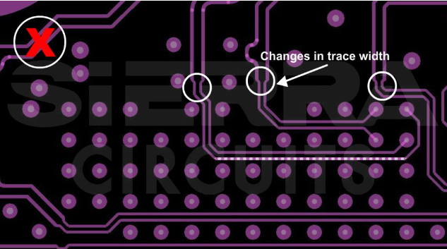
3. Signal Integrity and High-Speed Routing
With increasing clock speeds, signal integrity is a major concern. Reflections, crosstalk, and impedance mismatches can degrade performance.
Key Tips:
- Controlled Impedance Routing: Match trace impedance to the transmission line requirements (e.g., 50Ω for RF signals).
- Minimize Stub Lengths: Avoid long stubs in high-speed signals to prevent reflections.
- Differential Pair Routing: Route differential pairs (e.g., USB, HDMI) close together with consistent spacing.
- Avoid 90° Angles: Use 45° or curved traces to reduce signal reflections and EMI.
- Shielding and Grounding: Use ground planes beneath high-speed signals to minimize interference.
4. Grounding Strategies
Grounding mistakes are a common source of noise and interference in PCBs. A well-designed grounding scheme ensures stable operation.
Key Tips:
- Separate Analog and Digital Grounds: Use a single-point connection to avoid ground loops.
- Avoid Floating Grounds: Ensure all ground connections have a low-impedance return path.
- Use Ground Vias: In multilayer boards, connect ground planes with multiple vias to reduce inductance.
- Star Grounding for Mixed Signals: Useful in mixed-signal designs to prevent digital noise from coupling into analog circuits.
5. Thermal Management
Overheating can lead to component failure or degraded performance. Proper thermal design ensures long-term reliability.
Key Tips:
- Thermal Relief Pads: Use thermal relief connections for through-hole components to ease soldering and heat dissipation.
- Copper Pours for Heat Sinking: Increase copper area around high-power components to dissipate heat.
- Ventilation and Heatsinks: Ensure adequate airflow and use heatsinks for power components.
- Thermal Vias: Place vias under hot components to transfer heat to inner or bottom layers.
6. Design for Manufacturing (DFM)
A well-designed PCB should be easy to manufacture and assemble. Ignoring DFM guidelines can lead to costly revisions.
Key Tips:
- Follow Manufacturer’s Design Rules: Check minimum trace width, spacing, drill sizes, and annular ring requirements.
- Avoid Tombstoning: Ensure symmetrical pad sizes for small SMD components (e.g., resistors, capacitors).
- Silkscreen Clarity: Label components, pin 1 indicators, and polarity markings clearly.
- Test Points: Include test points for critical signals to facilitate debugging.
- Panelization: For small PCBs, consider panelization to reduce assembly costs.
7. EMI/EMC Considerations
Electromagnetic interference (EMI) can disrupt circuit operation and cause compliance failures. Proper design minimizes EMI risks.
Key Tips:
- Shield Sensitive Circuits: Use metal shields or grounded copper pour around RF and high-speed circuits.
- Filter Noisy Signals: Add ferrite beads or LC filters to suppress high-frequency noise.
- Minimize Loop Areas: Reduce the area between high-current traces and their return paths.
- Avoid Split Ground Planes: Unless necessary, keep ground planes solid to prevent antenna effects.
8. Testing and Debugging Techniques
Even the best-designed PCBs may have issues. Proactive testing and debugging save time and cost.
Key Tips:
- Use a Multimeter and Oscilloscope: Check power rails, signal integrity, and noise levels.
- In-Circuit Testing (ICT): Design test points for automated testing in production.
- Boundary Scan (JTAG): Useful for debugging complex digital circuits.
- Prototype Iterations: Test early prototypes to catch design flaws before mass production.
Conclusion
Mastering PCB design requires a combination of theoretical knowledge and hands-on experience. By applying these practical tips—smart component placement, proper power distribution, signal integrity techniques, effective grounding, thermal management, DFM, EMI reduction, and debugging—you can create high-performance, reliable, and manufacturable PCBs.
Whether you’re designing consumer electronics, industrial systems, or IoT devices, these best practices will help you avoid common pitfalls and optimize your PCB designs for success.