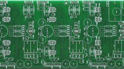
PCB design principles and circuit anti-interference measures rely on these few tricks
Printed circuit boards (PCBs) are the support for circuit components and devices in electronic products. It provides electrical connections between circuit components and devices. With the rapid development of electronic technology, the density of PCBs is getting higher and higher. The quality of PCB design has a great impact on the anti-interference ability.
Practice has proved that even if the circuit schematic is designed correctly, improper printed circuit board design will have an adverse effect on the reliability of electronic products. For example, if two thin parallel lines on the printed circuit board are close to each other, a delay in the signal waveform will be formed, and reflected noise will be formed at the terminal of the transmission line. Therefore, when designing printed circuit boards, attention should be paid to using the correct method, complying with the general principles of PCB design, and meeting the requirements of anti-interference design.

1.General principles of PCB design
In order to achieve the performance of electronic circuits, the layout of components and the layout of wires are very important. In order to design a high-quality and low-cost PCB, the following general principles should be followed:
2.Layout
First, consider the size of the PCB. When the PCB size is too large, the printed lines are long, the impedance increases, the anti-noise ability decreases, and the cost increases; if it is too small, the heat dissipation is poor and the adjacent lines are easily interfered. After determining the PCB size, determine the location of special components. According to the functional units of the circuit, all components of the circuit are laid out.
When determining the location of special components, the following principles should be followed:
(1) Shorten the connection between high-frequency components as much as possible, and try to reduce their distributed parameters and mutual electromagnetic interference. Components that are susceptible to interference should not be too close to each other, and input and output components should be kept as far away as possible.
(2) There may be a high potential difference between some components or wires, and the distance between them should be increased to avoid discharge leading to accidental short circuits. Components with high voltage should be placed as far as possible in places that are not easily touched by hands during debugging.
(3) Components weighing more than 15g should be fixed with a bracket and then soldered. Those large and heavy components that generate a lot of heat should not be installed on the printed circuit board, but should be installed on the chassis bottom plate of the whole machine, and heat dissipation should be considered. Thermistors should be kept away from heating components.
(4) The layout of adjustable components such as potentiometers, adjustable inductors, variable capacitors, and micro switches should take into account the structural requirements of the entire machine. If the adjustment is inside the machine, it should be placed in a convenient place on the printed circuit board; if the adjustment is outside the machine, its position should be consistent with the position of the adjustment knob on the chassis panel.
(5) Space should be reserved for the positioning holes on the printed circuit board and the space occupied by the fixing bracket.
According to the functional units of the circuit.
When laying out all the components of the circuit, the following principles should be followed:
(1) Arrange the positions of each functional circuit unit according to the flow of the circuit so that the layout is convenient for signal flow and the signal can maintain the same direction as much as possible.
(2) Take the components of each functional circuit as the center and lay out around it. The components should be arranged evenly, neatly, and compactly on the PCB. Try to reduce and shorten the leads and connections between components.
(3) For circuits working at high frequencies, the distribution parameters between components should be considered. Generally, the components of the circuit should be arranged in parallel as much as possible. This is not only beautiful, but also easy to assemble and solder, and easy to mass produce.
(4) Components located at the edge of the circuit board are generally not less than 2mm away from the edge of the circuit board. The shape of the circuit board is rectangular. The length and width are 3:2 or 4:3.
When the surface size of the circuit board is greater than 200×150mm, the mechanical strength of the circuit board should be considered. 2. Wiring
The wiring principles are as follows:
(1) The wires used for input and output terminals should be avoided as much as possible to be adjacent and parallel. Add ground wires between wires to avoid feedback coupling.
(2) The width of the printed circuit board wire is mainly determined by the adhesion strength between the wire and the insulating substrate and the current value flowing through them. When the copper foil thickness is 0.5mm and the width is 1~15mm, the temperature will not be higher than 3℃ when a current of 2A passes through. Therefore, a wire width of 1.5mm can meet the requirements. For integrated circuits, especially digital circuits, a wire width of 0.02~0.3mm is usually selected. Of course, as long as it is allowed, wide wires should be used as much as possible, especially power lines and ground wires. The spacing between wires is mainly determined by the insulation resistance and breakdown voltage between wires in the worst case. For integrated circuits, especially digital circuits, as long as the process allows, the spacing can be less than 5 to 8 mils.
(3) The bends of printed conductors are generally arc-shaped, while right angles or included angles will affect the electrical performance in high-frequency circuits. In addition, try to avoid using large-area copper foil, otherwise, the copper foil is prone to expansion and falling off when heated for a long time. When large-area copper foil must be used, use a grid shape. This is conducive to eliminating the volatile gas generated by the heat of the adhesive between the copper foil and the substrate.
1.Solder pad
The center hole of the solder pad should be slightly larger than the diameter of the device lead. A solder pad that is too large is prone to cold soldering. The outer diameter D of the solder pad is generally not less than (d+1.2) mm, where d is the lead hole diameter. For high-density digital circuits, the solder pad diameter can be (d+1.0) mm.
- PCB and circuit anti-interference measures
The anti-interference design of printed circuit boards is closely related to the specific circuits. Here we only explain several common measures for PCB anti-interference design. - Power line design
According to the current size of the printed circuit board, try to increase the width of the power line to reduce the loop resistance. At the same time, make the direction of the power line and the ground line consistent with the direction of data transmission, which helps to enhance the anti-noise ability. - Ground line design In the design of electronic products, grounding is an important method to control interference. If grounding and shielding can be used correctly, most interference problems can be solved. The ground line structure in electronic products generally includes system ground, chassis ground (shielded ground), digital ground (logic ground) and analog ground. The following points should be noted in the ground line design: (1) Correctly choose single-point grounding and multi-point grounding
In low-frequency circuits, the operating frequency of the signal is less than 1MHz, and its wiring and the inductance between devices have little effect, while the loop current formed by the grounding circuit has a greater impact on interference, so a single-point grounding method should be used. When the signal operating frequency is greater than 10MHz, the ground line impedance becomes very large. At this time, the ground line impedance should be reduced as much as possible, and multi-point grounding should be used nearby. When the operating frequency is between 1 and 10 MHz, if a single point grounding is used, the length of the ground wire should not exceed 1/20 of the wavelength, otherwise a multi-point grounding method should be used.
(2) Digital ground and analog ground are separated.
There are both high-speed logic circuits and linear circuits on the circuit board. They should be separated as much as possible, and the ground wires of the two should not be mixed. They should be connected to the ground wire of the power supply end respectively. The ground of the low-frequency circuit should be connected to the ground at a single point as much as possible. If the actual wiring is difficult, it can be connected in series and then connected in parallel. High-frequency circuits should adopt multi-point series grounding. The ground wire should be short and thick. A large area of grid-shaped ground foil should be used around high-frequency components as much as possible. The grounding area of the linear circuit should be increased as much as possible.
(3) The ground wire should be as thick as possible.
If the ground wire is a very thin line, the ground potential will change with the change of current, resulting in unstable timing signal level of electronic products and reduced anti-noise performance. Therefore, the ground wire should be as thick as possible so that it can pass three times the allowable current of the printed circuit board. If possible, the width of the ground wire should be greater than 3mm.
(4) The ground wire forms a closed loop.
When designing a ground wire system for a printed circuit board consisting only of digital circuits, making the ground wire a closed loop can significantly improve the anti-noise capability. The reason is that there are many integrated circuit components on the printed circuit board. Especially when there are components that consume a lot of power, due to the limitation of the thickness of the ground wire, a large potential difference will be generated on the ground wire, causing the anti-noise capability to decrease. If the ground wire forms a loop, the potential difference will be reduced, and the anti-noise capability of the electronic equipment will be improved. - Decoupling capacitor configuration
One of the common practices in PCB design is to configure appropriate decoupling capacitors at various key locations of the printed circuit board. The general configuration principle of decoupling capacitors is:
(1) A 10~100uf electrolytic capacitor is connected across the power input terminal. If possible, it is better to connect more than 100uF. (2) In principle, each integrated circuit chip should be equipped with a 0.01pF ceramic capacitor. If there is not enough space on the printed circuit board, a 1~10pF tantalum capacitor can be arranged for every 4~8 chips.
(3) For devices with weak noise immunity and large power supply changes when turned off, such as RAM and ROM memory devices, a decoupling capacitor should be directly connected between the power line and the ground line of the chip.
(4) The capacitor lead should not be too long, especially the high-frequency bypass capacitor should not have a lead.
In addition, the following two points should be noted:
(1) When there are contactors, relays, buttons and other components on the printed circuit board, they will generate large spark discharges when operating them, and an RC circuit must be used to absorb the discharge current. Generally, R is 1~2K and C is 2.2~47uF.
(2) The input impedance of CMOS is very high and is easily inductive, so the unused end should be grounded or connected to the positive power supply when in use.


