PCB Design Process Requirements for DFM Technology
Abstract
Design for Manufacturability (DFM) is a critical aspect of printed circuit board (PCB) design that ensures efficient, cost-effective, and reliable production. PCB designers must adhere to specific design process requirements to align with DFM principles, minimizing defects, reducing manufacturing costs, and improving yield. This paper explores the key PCB design process requirements for DFM, including material selection, trace and spacing rules, via design, component placement, thermal management, and testing considerations. By following these guidelines, designers can enhance manufacturability and optimize PCB performance.
1. Introduction
The PCB design process significantly impacts the manufacturability of a circuit board. DFM (Design for Manufacturability) focuses on designing PCBs in a way that simplifies fabrication and assembly while maintaining high quality. Poor design choices can lead to increased production costs, delays, and reliability issues. Therefore, understanding and implementing DFM-compliant design practices is essential for successful PCB manufacturing.
2. Material Selection and Stackup Design
2.1 Choosing the Right Substrate
The selection of PCB materials affects electrical performance, thermal stability, and manufacturability. Common materials include:
- FR-4: Standard material for most applications, offering good mechanical and electrical properties.
- High-Frequency Laminates: Used in RF and high-speed designs (e.g., Rogers, PTFE).
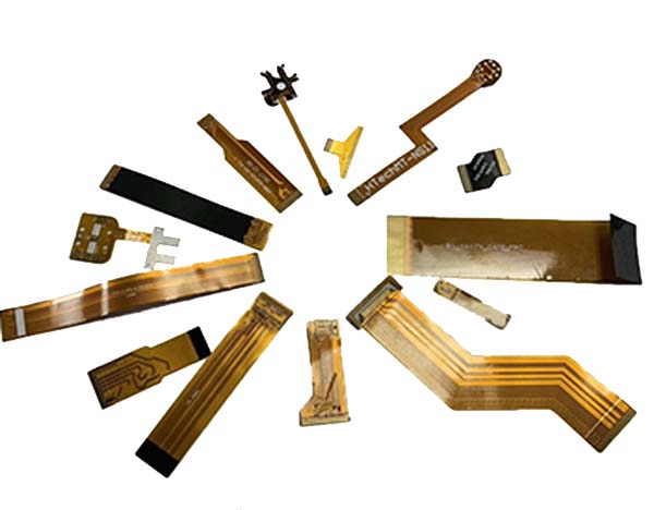
- Flexible Materials: Polyimide for flexible PCBs.
2.2 Stackup Configuration
A well-planned layer stackup ensures signal integrity and manufacturability:
- Symmetrical Stackups: Prevent warping during fabrication.
- Controlled Impedance Layers: Proper dielectric spacing for high-speed signals.
- Power and Ground Plane Placement: Reduces EMI and improves power distribution.
3. Trace and Spacing Rules
3.1 Minimum Trace Width and Spacing
DFM guidelines dictate minimum trace widths and clearances based on manufacturing capabilities:
- Standard PCBs: 5/5 mil (trace/space) for most fabricators.
- High-Density Designs: 3/3 mil or smaller, but increases cost.
- High-Current Traces: Wider traces to handle current without overheating.
3.2 Avoiding Acute Angles
- Use 45° or 90° angles to prevent acid traps in etching.
- Smooth Corners: Reduce signal reflections in high-speed designs.
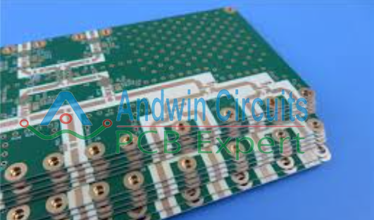
4. Via Design and Placement
4.1 Via Types and Sizing
- Through-Hole Vias: Standard for most PCBs.
- Blind/Buried Vias: Used in HDI (High-Density Interconnect) designs.
- Microvias: For ultra-high-density boards (laser-drilled).
DFM Considerations:
- Aspect Ratio: Via diameter vs. depth (typically ≤ 8:1 for reliable plating).
- Via-in-Pad: Requires filling and plating to prevent solder wicking.
- Thermal Relief Vias: Improve soldering for ground/power connections.
4.2 Via Placement Rules
- Avoid vias under BGA pads unless filled and capped.
- Keep vias away from board edges to prevent cracking.
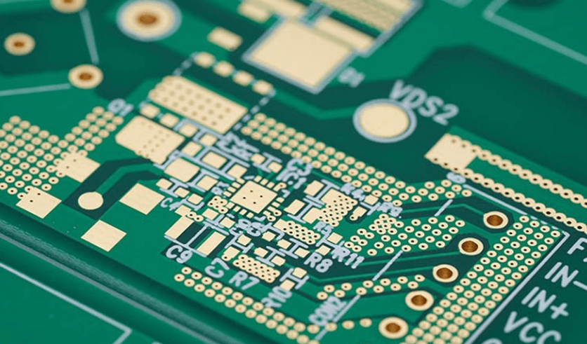
5. Component Placement and Footprint Design
5.1 Optimal Component Layout
- Group related components to minimize trace lengths.
- Consider assembly process: Avoid placing tall components near small ones.
- Orientation Consistency: Helps automated assembly (e.g., all polarized components facing the same direction).
5.2 Footprint Accuracy
- Follow IPC-7351 standards for pad sizes and spacings.
- Solder Mask Clearance: Prevents bridging during reflow.
- Silkscreen Legibility: Ensures clear component labeling.
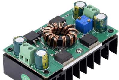
6. Thermal Management and Copper Balancing
6.1 Heat Dissipation Techniques
- Thermal Pads & Heat Sinks: For high-power components.
- Copper Pouring: Improves heat distribution.
- Via Arrays: Enhance thermal conductivity in multilayer boards.
6.2 Avoiding Warpage
- Balanced Copper Distribution: Prevents uneven thermal expansion.
- Symmetrical Layer Stackup: Reduces bending during reflow.
7. Solder Mask and Silkscreen Design
7.1 Solder Mask Requirements
- Adequate Clearance: Prevents solder bridging.
- Tented Vias: Protects against solder migration.
- Different Colors: Green is standard; other colors may require adjustments.
7.2 Silkscreen Best Practices
- Legible Text: Minimum font size ≥ 0.8mm.
- Avoid Overlapping Pads: Ensures readability after assembly.
8. Testing and Design Validation
8.1 Design Rule Checks (DRC)
- Automated DRC Tools: Verify spacing, trace width, and via placement.
- Manufacturing Feedback: Collaborate with fabricators early.
8.2 Testability Considerations
- Test Points: Include accessible pads for in-circuit testing (ICT).
- Flying Probe Compatibility: Ensure probe access for bare-board testing.
9. Conclusion
Adhering to DFM principles in PCB design ensures manufacturability, reduces costs, and improves reliability. Key considerations include material selection, trace and via design, component placement, thermal management, and testing strategies. By integrating DFM early in the design process, engineers can optimize PCB production and minimize post-fabrication issues.