PCB Design – Setting Up Routing Constraint Conditions
Introduction
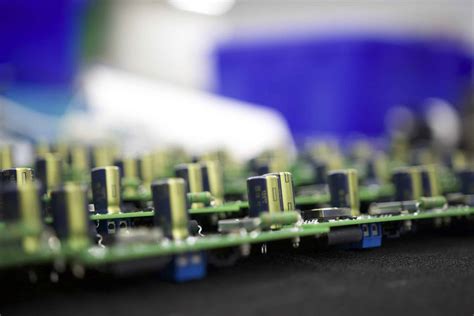
Printed Circuit Board (PCB) design has evolved significantly with the increasing complexity of electronic devices. One of the most critical aspects of modern PCB design is establishing proper routing constraint conditions. These constraints ensure signal integrity, manufacturability, and reliability of the final product. This 2000-word article explores the various types of routing constraints, their importance, and best practices for implementation in PCB design.
Understanding Routing Constraints
Routing constraints in PCB design refer to the set of rules and limitations that govern how traces (electrical connections) are placed and routed on a PCB. These constraints are typically defined in the PCB design software and enforced throughout the design process.
Why Routing Constraints Matter
- Signal Integrity: Proper constraints maintain signal quality by controlling impedance, crosstalk, and reflections.
- Manufacturability: Constraints ensure the design can be reliably produced within manufacturing capabilities.
- Performance: They help achieve the desired electrical performance of the circuit.
- Reliability: Proper constraints reduce the likelihood of field failures.
- Design Efficiency: They automate many routing decisions, speeding up the design process.
Types of Routing Constraints
1. Physical Constraints
Physical constraints define the geometric limitations of the PCB traces:
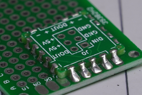
- Trace Width: Minimum and maximum allowable widths for different nets
- Clearance: Minimum spacing between traces, pads, and vias
- Via Size: Specifications for via diameters and hole sizes
- Layer Usage: Which layers can be used for specific types of routing
2. Electrical Constraints
These constraints ensure proper electrical performance:
- Impedance Control: Maintaining specific impedance values for critical traces
- Length Matching: Ensuring certain traces have equal or proportional lengths
- Differential Pair Routing: Special rules for differential signals
- Current Capacity: Ensuring traces can handle required current loads
3. Manufacturing Constraints
Constraints related to PCB fabrication and assembly:
- Manufacturing Tolerances: Accounting for fabrication process limitations
- Solder Mask Clearance: Space around pads for proper solder mask application
- Silkscreen Requirements: Text and marking placement rules
4. High-Speed Design Constraints
Special constraints for high-frequency designs:
- Controlled Impedance Routing: Precise trace geometry for impedance matching
- Length Tuning: Adjusting trace lengths to meet timing requirements
- Crossing Plane Splits: Rules for traces crossing power plane divisions
Setting Up Routing Constraints in PCB Design Software
Step 1: Define Design Requirements
Before entering constraints into the software, gather all requirements:
- Electrical specifications (impedance, current requirements)
- Mechanical specifications (board thickness, layer stackup)
- Manufacturing capabilities (minimum trace/space, via sizes)
- Signal integrity requirements (for high-speed designs)
Step 2: Create Constraint Classes
Most PCB design software allows creating classes or groups of nets with similar requirements:
- Power Nets: Typically require wider traces
- Signal Nets: May have various subgroups based on speed
- Clock Signals: Often have strict length and routing requirements
- Differential Pairs: Require matched length and spacing

Step 3: Specify Physical Constraints
For each class, define:
- Minimum and Preferred Trace Widths
- Power traces: 10-50 mils or more depending on current
- Signal traces: Typically 4-10 mils
- High-current traces: Calculate based on current requirements
- Clearance Rules
- Trace-to-trace
- Trace-to-pad
- Trace-to-via
- Pad-to-pad
- Via Specifications
- Drill size
- Pad size
- Via type (through-hole, blind, buried)
Step 4: Establish Electrical Constraints
- Impedance Control
- Define target impedance (e.g., 50Ω single-ended, 100Ω differential)
- Specify which layers and trace widths achieve this
- Length Matching
- Set tolerance for matched length groups (e.g., ±50 mils)
- Define matching topology (e.g., serpentine tuning)
- Differential Pair Rules
- Coupling requirements
- Maximum separation
- Length matching tolerance
Step 5: Configure High-Speed Constraints
For high-speed designs:
- Topology Rules
- Define preferred routing patterns
- Set stub length limitations
- Timing Constraints
- Propagation delay requirements
- Flight time matching
- EMI Considerations
- Return path rules
- Shielding requirements
Best Practices for Constraint Management
1. Hierarchical Constraint Organization
Create a logical hierarchy of constraints:
- Global Defaults: Apply to all nets unless overridden
- Class-Level Rules: Apply to groups of nets
- Net-Specific Exceptions: For unique requirements
2. Use of Constraint Templates
For organizations designing multiple similar boards:
- Create template constraint sets
- Store approved constraint profiles
- Reuse across projects to maintain consistency
3. Constraint Verification
Regularly verify that constraints are:
- Complete (all critical nets have appropriate rules)
- Correct (rules match design requirements)
- Consistent (no conflicting rules)
4. Documentation
Maintain thorough documentation of:
- Constraint rationale (why each rule exists)
- Revision history
- Exception approvals
Common Constraint Challenges and Solutions
Challenge 1: Conflicting Requirements
Solution: Establish priority rules and exception handling procedures.
Challenge 2: Constraint Overload
Solution: Avoid excessive constraints that make routing impossible. Focus on critical requirements.
Challenge 3: Manufacturing Changes
Solution: Maintain close communication with fabricators and update constraints accordingly.
Challenge 4: Legacy Designs
Solution: Carefully document constraint changes when updating older designs.
Advanced Constraint Techniques
1. Conditional Constraints
Rules that change based on context:
- Different clearances for adjacent signals
- Variable width traces (tapering)
2. 3D Constraints
Accounting for:
- Component height restrictions
- Mechanical interference
- Thermal considerations
3. Flex/Rigid-Flex Constraints
Special rules for flexible circuits:
- Bend radius requirements
- Stiffener areas
- Transition zones
Constraint Management in Different PCB Design Tools
While concepts are similar, implementation varies by software:
- Altium Designer: Uses “PCB Rules and Constraints Editor”
- Cadence Allegro: Utilizes “Constraint Manager”
- Mentor Xpedition: Implements “Constraint Editor”
- KiCad: Employs “Design Rules” settings
Future Trends in Constraint Management
- AI-Assisted Constraint Generation: Automatic suggestion of constraints based on design intent
- Cloud-Based Constraint Libraries: Shared constraint repositories for organizations
- Real-Time Constraint Analysis: Instant feedback during routing
- 3D-Aware Constraints: More sophisticated mechanical integration
Conclusion
Proper setup of routing constraint conditions is fundamental to successful PCB design. By systematically defining and managing physical, electrical, and manufacturing constraints, designers can ensure their boards meet all requirements while remaining manufacturable and reliable. As PCB technology continues to advance with higher speeds and densities, constraint management will only grow in importance. Investing time in establishing a robust constraint system early in the design process pays dividends throughout the product development cycle, reducing errors, iterations, and time-to-market.
Effective constraint management requires both technical knowledge of PCB design requirements and familiarity with the capabilities of your design software. By following the practices outlined in this article and staying current with evolving constraint management technologies, PCB designers can consistently produce high-quality, high-performance circuit boards.