PCB Design Steps that Impact Manufacturing
Before becoming an engineer,I spent a lot of time trying to develop product designed by others.These included automobiles,appliances,and electronic devices.The most frustrating aspect of repair work is when routine or preventative maintenance tasks are extremely comp[ex or difficult to perform.Often,the tasks that must be done are the easiest to implement and execute,If this isn’t the case,it’s clear that the designer has given little thought to the designer has given little thought to the fact that someone well have to perform these so-called routine tasks in the future.The consequences of this”oversight”can be significant,leading to excessive downtime,reduced production,and lost revenue.
Even more serious than not considering routine maintenance and repair is not considering manufacturing during design,Doing so can negatively impact board functionality and manufacturability.Such omissions can result in redesigns,PCB rework,singificant turnaround times and unnecessary manufacturing costs.Therefore,it’s essential to consider how design choices impact board manufacturing.Let’s review circuit board design and outline a set of PCB design steps to illustate the key areas where manufacturing impacts need to be considered.
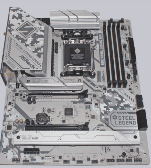
How PCB Design Steps Impact Manufacturing Creating a concept or a set of performance goals and creating a design that can be physically realized is no easy task.Becoming a good PCB designer requires years of experience,and even then ,new PCB design software,component ,and technologies are always available.Therefore,circuit board design is career-long learning experience.One aspect you should understand early in is the need for synchronization between design specification and PCB fabrication.Understanding how design decisions impact PCB fabrication should be a reference throughout the design process,below is a checklist of PCB design steps that will help your contract manufacturer(CM)build your board.
PCB Design Step 1:Select the Fewest Unique Component
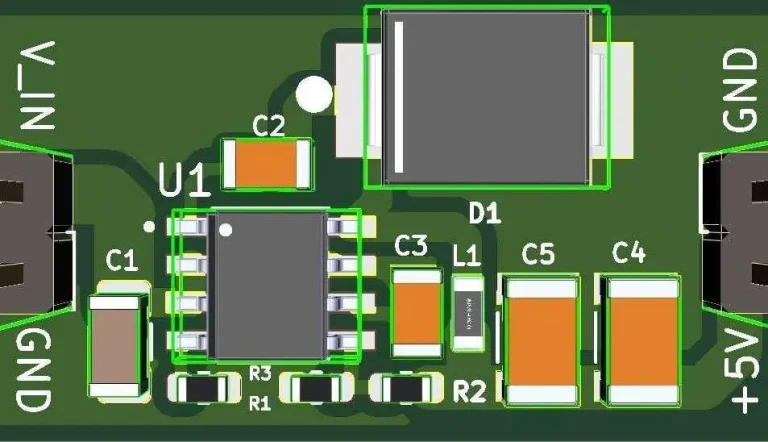
Whenever possible,choose similar components.This facilitates the pick-and-place process.Using Packages of the same size for multiple component is also helpful.
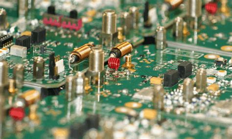
PCB Design Step 2:Use SMDs and Minimize Through-Hole Components
SMDs and through-hole components require different soldering methods,with through-hole component requiring a longer process.
PCB Design step 3:Don’t Overload Nets
Nets with a large number of component connections on the schematic translate into wider traces or heavier copper weights on your layout.This can lead to issued with layer and overall board size.
PCB Design step 4:Follow CM Clearance Guidelines
One,if not the other,main reason to ensure adequate clearance between board components is solder resist,This is a fundamental manufacturing task that protects your board and helps isolate electrical connections that must be soldered during the PCB soldering process.
PCB Design step 5:Avoid Board-Edge
Connectors Whenever possible
Just like elsewhere in your PCB layout,board-edge clearance is important.There’s a tendency(and sometimes necessity)to place connectors near or just above the board edge.However,doing so requires good panelization and consultation with your CM.
PCB Design Step 6:Use Sufficient,But Minimal.Layers for Stackup
The more layers you have,the more material and processing time your CM will require,However,you stackup to meet your signal and ground needs.
PCB Design Step7:Use Minimal Routing Complexity
Since most of your designs will likely be multilayer,how best to route your vias is a major design and manufacturing issue,The most important rule of thumb in manufacturing is that more complexity is better.PCB Design
Step 8:Perform Frequent Design for Component(DFM)checks
Perhaps the most important thing you can do during the design process is to frequently perform Design for Components(DFM)checks on your circuit.However,constraints should be based on your CM’s rules and guidelines.
PCB Design step9: Perform Thermal Analysis and PDN Checks
It is also important to simulate your board and analyze its thermal response and PDN.Excessive temperatures on components or distribution boards can cause problems,especially during soldering during PCB assembly.
PCB Design Step 10:Ensure the Manufacturing file Package is complete and Accurate last but not least
you should ensure that design specifications and all relevant data,information,and drawing are included with your product.
Design files must be incorporated into the PCB design steps designed to support the board manufacturing process.Failure to do so will result in redesigns,long turnaround times,and potentially unnecessary cost,Choosing comprehensive and user-friendly PCB design software can also greatly assist with PCB manufacturing.