PCB design tips
PCB Design
Introduces the basic principles of printed circuit board design, such as when to design a single-sided board, double-sided board or multi-layer board; as well as the coordinate system, design magnification ratio, production conditions of printed circuits, and PCB standardization documents during PCB design

I. Types of printed circuit boards
Single-sided printed circuit boards are widely used in civilian electronic products, such as radios, tape recorders, televisions, and electronic game consoles. Its manufacturing cost is the lowest among all types of printed circuit boards. Single-sided printed circuit boards may also be used in industrial electronic products. Mainly based on the complexity and density of the circuit and the assembly requirements of the whole machine, a single-sided printed circuit board should be used when all interconnections can be completed on a single side.
(1) In the case where a single-sided printed circuit board cannot complete all interconnections of the circuit, it is necessary to consider designing a double-sided printed circuit board.
Most double-sided printed circuit boards use metallized holes to achieve through-connection of wires on both sides. In a few cases, non-metallized holes can also be used for double-sided printed circuit boards. Its through-connection is mainly achieved by inserting component leads into the holes.
In the following cases, consider designing a multilayer printed circuit board:
1) Double-sided printed circuit boards cannot complete all the interconnections of the circuit, and more jumper wires need to be added.
2) Light weight and small size are required.
3) There are high-speed circuits.
Since the interconnection wires of multilayer printed circuit boards are short, the attenuation of high-speed pulse signals is reduced; the ground layer of the multilayer printed circuit board can provide good shielding for the high-speed signal layer; the high-frequency distributed capacitance between the ground layer and the power layer has a good decoupling effect on the power supply.
4) High reliability is required.
Several double-sided printed circuit board assemblies can be combined into a multilayer board assembly to improve the reliability of the entire electronic product.
5) Simplify the layout of printed circuit boards and the design of photographic base maps.
Some double-sided printed circuit board layouts are very complex due to the interconnection. After using multilayer printed circuit boards, the power or ground wire can be separated from the signal wire to solve the problem, that is, the power layer and the ground layer are set separately, or the power layer and the ground layer are laid on the same layer.
In order to meet the needs of certain special assembly of electronic equipment and reduce weight and increase assembly density, it is sometimes required to use flexible printed circuits or flexible-rigid combined printed circuits. Flexible printed circuits can also be used as connecting cables, saving time for welding single wires and eliminating assembly errors. Flexible printed circuits can also be used for mobile electronic components.
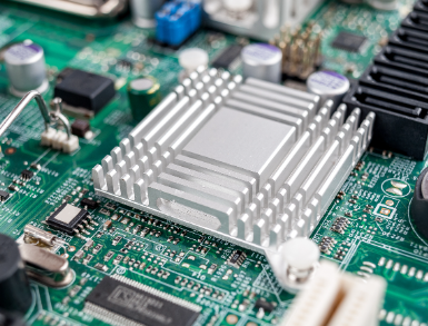
When the conductors of the printed circuit board are subject to large currents or the power consumption of the entire printed circuit board is very large, causing it to exceed the allowable operating temperature, it is necessary to design a printed circuit board with a metal core or surface heat sink.
When a printed circuit board is used to make a rotary switch or a contact encoder disk, a flush printed circuit should be designed.

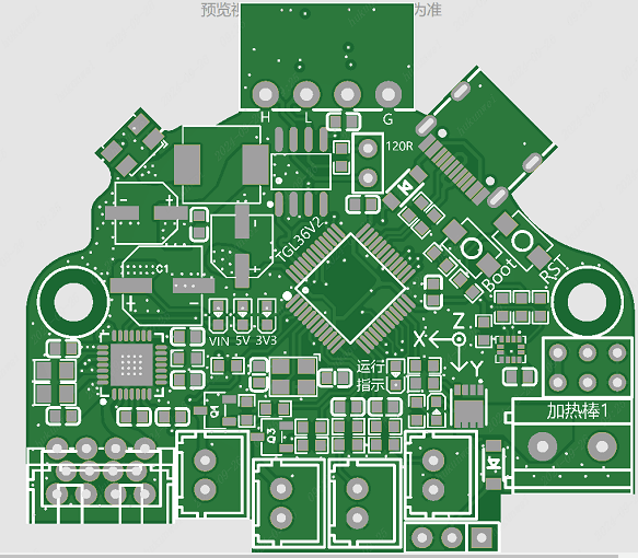
(2) Coordinate network system
When designing a printed circuit board, a commonly followed coordinate network system should be used. The leads of the components are inserted exactly into the assembly holes located at the intersection of the grid.
According to the specified grid, computer-aided design (CAD) systems, automatic photolithography machines, CNC drilling devices, computer-aided testing (CAT) systems, and component automatic insertion devices can easily compile or automatically generate control programs. For manual layout of printed circuit board sketches and production of photographic base maps, the use of a coordinate grid system is also convenient for calculation and operation.
According to the national standard “Printed Circuit Grid System” GB1360-1998, the grid spacing of the basic grid is 2.5mm. If necessary, an auxiliary grid can be set, and its grid spacing is 1, 2 (i.e. 1.25mm) or 1/4 (i.e. 0.625mm) of the basic grid. For printed circuit boards for integrated circuits with a center distance of 2.54mm between adjacent leads, a 2.54mm basic grid can be used. The 2.54mm basic grid system also has two auxiliary grids with spacings of 1.27mm and 0.635mm.
(3) Design magnification ratio
According to the requirements of the dimensional accuracy of the printed circuit board, the photographic base map is produced at a ratio of 1:1, 2:1 or even 4:1. The layout sketch of the printed circuit board is also drawn at the same ratio. This can prevent the re-drawing of the enlarged layout sketch when making the photographic base map, and it is also convenient for checking the photographic base map.
The most commonly used magnification ratio for layout sketches or photographic bases is 2:1. The wiring accuracy is relatively high and the operation is relatively convenient according to this ratio. The magnification ratio of 4:1 is only used when the precision requirements of the printed board are particularly high or when a high-precision conductive pattern program is input and compiled using a digital instrument. Designing layout sketches at a ratio of 1:1 is only suitable for relatively simple double-sided printed circuit boards or the power layer and ground layer of multi-layer printed circuit boards.
(4) Production conditions of printed circuits
When designing printed circuit boards, production conditions should be considered and familiar. For example: methods for making photographic plates (photographic reduction method, photolithography method, 1:1 mapping method, etc.), the maximum base size allowed by the phototypesetting machine, the maximum and minimum sizes of printed circuit boards processed by various equipment, the drilling accuracy of the drilling machine, the requirements for punching and cutting, fine wire pattern printing technology and etching accuracy, etc.
(5) Standardization
The result of standardization is that the printed circuit board production process can be simplified, the production cycle can be shortened, the cost can be reduced, and the quality control requirements of the printed circuit board can be met. Therefore, designers must apply and strictly abide by these standards.
Applicable standards include the national standard (GB), the International Electrotechnical Commission (IEC TC52), the US Military Standard (MIL), the British Standard (BS), the Japanese Industrial Standard (JIS) and the Japan Printed Circuit Association (JPCA) and other relevant standards.
(6) Design documents
- Circuit diagram (electrical schematic diagram)
In addition to using the common method to indicate the connection relationship of the circuit, the circuit diagram must also mark certain special parts according to the design requirements of the printed circuit board.
For example: the relationship between the input and output terminals of the printed circuit board and the connector, the length of the key signal line, the wire protected by the ground wire, the wire of special width, the device that generates electromagnetic interference, the components that generate a lot of heat, and the thermistor components, etc. - Component table
The component table includes all the resistors, capacitors, transistors, diodes, integrated circuits, transformers, inductors, heat sinks and metal parts in the circuit diagram. In the component table, the corresponding numbers in the circuit diagram (such as R1, R2, R3, …, C1, C2, C3 …), the specifications of the components, the matching requirements of the metal parts, the mechanical dimensions, etc., should be indicated. If necessary, physical components should be used as reference. - Component wiring table
This table is generally used in CAD automatic wiring, and it only indicates the connection relationship between various components. - Mechanical processing drawing
The mechanical processing drawing is an important document for mechanical processing of printed circuit boards. The mechanical processing drawing includes the following parts:
1) The overall dimensions and deviations of the printed circuit board, including the dimensions and deviations of the printed plug part, the dimensions of the mechanical mounting holes, and the dimensions and deviations between them and the reference datum.
2) The name, symbol, thickness and thickness of the copper-clad laminate used. Sometimes the thickness of the insulating substrate between the copper foils is more emphasized.
3) Technical requirements for surface plating, such as the thickness of tin-lead plating, the tin-lead ratio, the thickness of nickel or gold plating, etc.
4) Surface coating requirements, such as solderability coating, solder mask coating, etc.
5) Assembly drawings and component tables are both essential documents for printed circuit board electrical assembly. The assembly drawing should clearly mark the installation position of the components, the names of the components and their polarity, etc.