Pcb designators
Understanding Common PCB Designators
Printed Circuit Boards (PCBs) are the backbone of modern electronic devices, serving as the platform upon which electronic components are mounted and interconnected. Understanding common PCB designators is crucial for anyone involved in the design, manufacturing, or repair of electronic circuits. These designators are alphanumeric codes that identify the various components on a PCB, ensuring clarity and consistency in documentation and communication.
To begin with, PCB designators typically consist of a letter followed by a number.
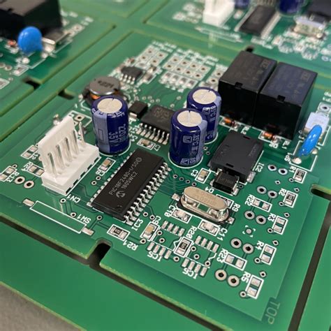
The letter indicates the type of component, while the number provides a unique identifier for each instance of that component type on the board. For example, “R1” might denote the first resistor, while “C2” could represent the second capacitor. This systematic approach allows for easy identification and reference, which is essential for troubleshooting and assembly.
Resistors, one of the most common components, are usually designated with the letter “R.”
Capacitors, which store electrical energy, are identified by the letter “C.” Inductors, used for their ability to store energy in a magnetic field, are marked with the letter “L.” These basic components form the foundation of most electronic circuits, and their designators are universally recognized.
Transistors, which act as switches or amplifiers, are typically labeled with the letter “Q.”
Integrated Circuits (ICs), which can perform a variety of functions depending on their design, are designated with the letter “U.” Diodes, which allow current to flow in one direction only, are marked with the letter “D.” These components are more complex than basic passive components like resistors and capacitors, and their designators help in identifying their specific roles within the circuit.
Furthermore, connectors, which provide a means to connect the PCB to external devices or other PCBs, are usually designated with the letter “J.”
Switches, used to open or close electrical circuits, are marked with the letter “S.” Crystals and oscillators, which provide precise timing signals, are identified by the letter “Y.” These components are essential for the functionality and connectivity of the PCB, and their designators ensure that they are correctly identified and placed.
In addition to these common designators, there are also specialized ones for less frequently used components.
For instance, transformers, which transfer electrical energy between circuits, are designated with the letter “T.” Fuses, which protect circuits from overcurrent, are marked with the letter “F.” Relays, which are electrically operated switches, are identified by the letter “K.” These specialized components play critical roles in specific applications, and their designators help in maintaining clarity in complex designs.
Moreover, understanding PCB designators is not only important for those who design and build PCBs but also for those who maintain and repair them. Accurate identification of components ensures that replacements are correct and that the circuit functions as intended. It also facilitates effective communication between engineers, technicians, and other stakeholders involved in the lifecycle of the electronic device.
In conclusion, PCB designators are an essential aspect of electronic circuit design and maintenance. They provide a standardized method for identifying and referencing components, ensuring clarity and consistency across various stages of a PCB’s lifecycle. By familiarizing oneself with these common designators, one can enhance their understanding and efficiency in working with electronic circuits. This knowledge is indispensable for anyone involved in the field of electronics, from designers and manufacturers to repair technicians and engineers.

Best Practices for Labeling PCB Designators
In the realm of printed circuit board (PCB) design, the meticulous labeling of PCB designators is a critical practice that ensures clarity, efficiency, and accuracy throughout the development and manufacturing processes. PCB designators, also known as reference designators, are alphanumeric codes assigned to each component on a PCB to uniquely identify them. Adhering to best practices for labeling these designators is essential for maintaining a streamlined workflow and avoiding costly errors.
To begin with, it is imperative to adopt a standardized naming convention for PCB designators.
This convention typically involves a combination of letters and numbers, where the letter represents the type of component and the number provides a unique identifier. For instance, resistors might be labeled as R1, R2, R3, and so forth, while capacitors could be designated as C1, C2, C3, etc. This systematic approach not only facilitates easy identification but also aids in the quick location of components during assembly and troubleshooting.
Moreover, consistency in labeling is paramount.
Ensuring that the same naming convention is applied uniformly across all design files and documentation helps prevent confusion and misinterpretation. This consistency extends to the use of uppercase letters for designators, as lowercase letters can be easily misread, leading to potential errors. Additionally, avoiding the use of special characters or spaces in designators is advisable, as these can cause issues with certain software tools and databases.
Another best practice involves the strategic placement of designators on the PCB layout.
Designators should be positioned in a manner that is both readable and non-intrusive. Placing them too close to component pads or traces can obscure important details and complicate the assembly process. Conversely, placing them too far away from their respective components can lead to ambiguity. Therefore, it is essential to strike a balance, ensuring that designators are clearly visible without interfering with other elements of the PCB.
Furthermore, the use of silkscreen layers for designators is highly recommended.
The silkscreen layer, typically printed on the top and bottom surfaces of the PCB, provides a visual guide for component placement and orientation. Including designators on the silkscreen layer enhances the readability and accessibility of the PCB, particularly during manual assembly and inspection. However, it is crucial to ensure that the silkscreen does not overlap with solder pads or vias, as this can affect the soldering process and lead to defects.
In addition to these practices, leveraging design automation tools can significantly enhance the accuracy and efficiency of labeling PCB designators.
Modern PCB design software often includes features that automatically generate and place designators based on predefined rules. Utilizing these tools can help maintain consistency and reduce the likelihood of human error. However, it is still important to review and verify the automatically generated designators to ensure they meet the specific requirements of the project.
Lastly, thorough documentation is an integral aspect of best practices for labeling PCB designators.
Comprehensive documentation should include a detailed bill of materials (BOM) that lists all components along with their corresponding designators. This documentation serves as a vital reference for all stakeholders involved in the project, from designers and engineers to manufacturers and quality assurance teams. Clear and accurate documentation facilitates effective communication and collaboration, ultimately contributing to the successful realization of the PCB design.
In conclusion, adhering to best practices for labeling PCB designators is essential for ensuring the clarity, efficiency, and accuracy of the PCB design process. By adopting standardized naming conventions, maintaining consistency, strategically placing designators, utilizing silkscreen layers, leveraging automation tools, and providing thorough documentation, designers can significantly enhance the quality and reliability of their PCB projects.

The Importance of Consistent PCB Designators in Manufacturing
In the realm of electronics manufacturing, the importance of consistent PCB designators cannot be overstated. Printed Circuit Boards (PCBs) serve as the backbone of electronic devices, providing the necessary pathways for electrical currents to flow between various components. The designators, which are alphanumeric codes assigned to each component on a PCB, play a crucial role in ensuring that the manufacturing process is both efficient and error-free. These designators, such as R1 for a resistor or C1 for a capacitor, provide a standardized method for identifying components, thereby facilitating clear communication among engineers, manufacturers, and quality control teams.
One of the primary reasons for maintaining consistency in PCB designators is to minimize the risk of errors during the assembly process.
When designators are used consistently, it becomes easier for assembly line workers to identify and place components accurately. This reduces the likelihood of incorrect placements, which can lead to malfunctioning devices and costly rework. Furthermore, consistent designators streamline the process of cross-referencing components with the Bill of Materials (BOM), ensuring that the correct parts are used at each stage of production. This alignment between the PCB layout and the BOM is essential for maintaining the integrity of the final product.
In addition to reducing errors, consistent PCB designators enhance the efficiency of troubleshooting and maintenance.
When a device malfunctions, engineers often rely on schematics and PCB layouts to diagnose the issue. Consistent designators allow for quick identification of components, making it easier to trace electrical pathways and pinpoint faults. This is particularly important in complex circuits where multiple components interact in intricate ways. By facilitating faster and more accurate diagnostics, consistent designators contribute to reduced downtime and lower maintenance costs.
Moreover, the use of consistent PCB designators supports effective communication across different teams and stakeholders involved in the manufacturing process.
Engineers, designers, and production staff often work in tandem to bring a product from concept to reality. Clear and consistent designators ensure that everyone is on the same page, reducing the potential for misunderstandings and miscommunications. This is especially critical in large-scale manufacturing operations where multiple teams may be working on different aspects of the same project. Consistency in designators fosters a common language that enhances collaboration and coordination.
Another significant benefit of consistent PCB designators is their role in quality control and assurance.
During the inspection phase, quality control teams rely on designators to verify that each component is correctly placed and soldered. Consistent designators make it easier to conduct thorough inspections, as inspectors can quickly locate and check each component against the design specifications. This not only ensures that the final product meets the required standards but also helps in identifying any deviations or defects early in the process.
Furthermore, consistent PCB designators are invaluable in the context of documentation and record-keeping.
Accurate records of PCB layouts, including designators, are essential for future reference, whether for product updates, repairs, or regulatory compliance. Consistent designators ensure that these records are clear and unambiguous, facilitating easier retrieval and interpretation of information.
In conclusion, the importance of consistent PCB designators in manufacturing cannot be emphasized enough. They play a pivotal role in minimizing errors, enhancing troubleshooting efficiency, supporting effective communication, ensuring quality control, and maintaining accurate documentation. By adhering to a standardized approach to PCB designators, manufacturers can achieve higher levels of precision, efficiency, and reliability in their production processes, ultimately leading to superior electronic products.
How to Avoid Common Mistakes with PCB Designators
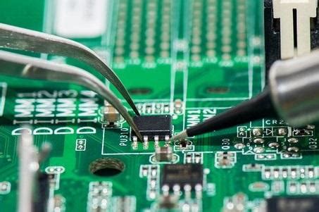
Printed Circuit Board (PCB) designators are essential elements in the design and manufacturing process of electronic circuits. They serve as unique identifiers for each component on a PCB, ensuring that assembly, testing, and troubleshooting can be conducted efficiently. However, despite their importance, common mistakes with PCB designators can lead to significant issues, ranging from minor inconveniences to critical failures. To avoid these pitfalls, it is crucial to understand the best practices and common errors associated with PCB designators.
One of the most frequent mistakes is the inconsistent use of designators.
Inconsistency can arise from various sources, such as using different naming conventions or failing to follow a standardized format. For instance, some designers might label resistors as “R1, R2, R3,” while others might use “R01, R02, R03.” This lack of uniformity can cause confusion during the assembly process, leading to potential misplacements or incorrect installations. To mitigate this risk, it is advisable to establish and adhere to a standardized naming convention from the outset of the design process.
Another common error is the omission of designators altogether.
This oversight can occur when designers are focused on the schematic and layout aspects of the PCB and inadvertently neglect to assign designators to each component. The absence of designators can severely hinder the assembly and testing phases, as technicians will struggle to identify and place components accurately. To prevent this, designers should incorporate a systematic review process to ensure that all components are appropriately labeled before finalizing the design.
Furthermore, the placement of designators on the PCB layout is a critical consideration.
Poor placement can result in designators being obscured by components or solder joints, making them difficult to read during assembly and inspection. To avoid this, designers should strategically position designators in clear, unobstructed areas of the PCB. Additionally, using a consistent font size and style can enhance readability and reduce the likelihood of errors.
Another aspect to consider is the duplication of designators.
This mistake often occurs when components are copied and pasted within the design software, leading to multiple instances of the same designator. Duplicate designators can create significant confusion and errors during the assembly process, as it becomes unclear which component corresponds to which designator. To address this issue, designers should utilize design software features that automatically check for and prevent duplicate designators.
Moreover, it is essential to consider the impact of design changes on PCB designators.
As designs evolve, components may be added, removed, or repositioned, necessitating updates to the designators. Failing to update designators in response to these changes can result in outdated or incorrect information being conveyed to the assembly team. To ensure accuracy, designers should implement a robust change management process that includes regular reviews and updates of designators.
In addition to these considerations, effective communication with the assembly team is paramount. Providing clear and comprehensive documentation, including a Bill of Materials (BOM) and assembly drawings with well-labeled designators, can significantly reduce the likelihood of errors. Engaging in regular communication with the assembly team can also help identify potential issues early and facilitate prompt resolution.
In conclusion, avoiding common mistakes with PCB designators requires a combination of standardized practices, careful attention to detail, and effective communication. By adhering to these principles, designers can enhance the accuracy and efficiency of the PCB assembly process, ultimately leading to higher-quality electronic products.