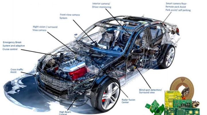
PCB desmearing and hole conditioning process
1.Conditioning
This word refers to the “conditioning” or “adaptation” of the board itself in a broad sense, so that it can adapt to the subsequent conditions. In a narrow sense, it means that the dry board and hole wall are made “hydrophilic” and “positively charged” before entering the PTH process, and the cleaning work is completed at the same time, so that other subsequent treatments can be continued. This action of tidying up the hole wall before starting the through-hole process is called hole conditioning.

2.Desmearing
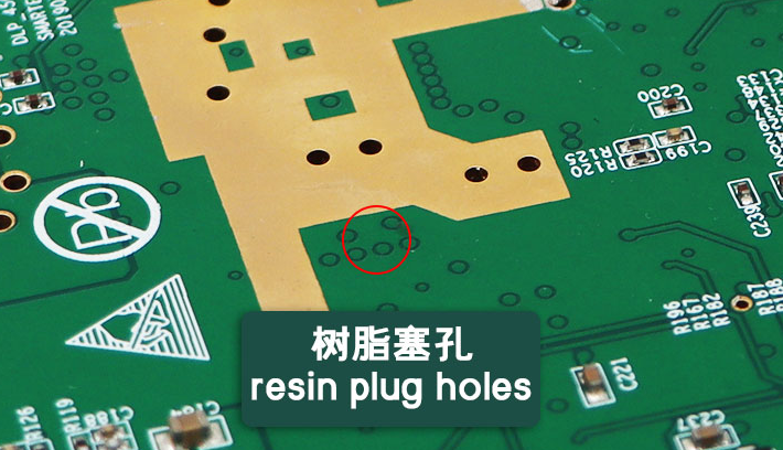
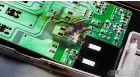
It means that when the circuit board is in the high friction heat of drilling, when its temperature exceeds the Tg of the resin, the resin will soften or even form a fluid and cover the hole wall with the rotation of the drill bit. After cooling, it forms a fixed glue paste residue, which forms a barrier between the inner copper hole ring and the copper hole wall made later. Therefore, at the beginning of PTH, various methods should be used to remove the formed glue residue to achieve the purpose of subsequent good connection. The attached figure shows that the glue residue has not been completely removed, leaving a gap between the copper hole wall and the inner hole ring that cannot be connected.
3.Dichromate
Refers to Cr2O7, and common ones are K2Cr2O7, (NH4)2Cr2O7, etc. Because there are two chromium atoms in its molecular formula, it is called “heavy” (ㄔㄨㄥ′) chromate to distinguish it from chromate (CrO ). In the circuit board industry, the desmearing process before PTH used a high concentration of potassium dichromate (900 g/l) bath solution in the early years. This strong oxidant was used as a chemical to remove glue residue from the hole wall. In addition, the fixed screen used for single-panel printing also has a photosensitive chemical “ammonium dichromate” added to the screen cloth photosensitive emulsion, which is often referred to as Dichromate in the industry. In recent years, due to the improvement of environmental awareness, this notorious “hexavalent chromium” is not only extremely harmful to the ecological environment, but also has the risk of causing cancer. Therefore, it has long become the target of public criticism and is no longer used by the industry.
4.Etchback
It refers to the process of deliberately etching away the resin and fiberglass substrate between the copper ring layers on the through-hole walls of multi-layer PCB boards by about 0.5 to 3 mil. This process allows the annular rings of each copper layer to protrude slightly into the hole. After PTH and subsequent two copper platings to obtain the copper hole wall, the hole copper can be formed to be firmly connected with the annular rings of each layer in a three-sided clamping manner. This “etch back” was a special requirement of the US military specification MIL-P-55110 for multi-layer PCB boards in the early days.
However, after many years of practical experience, it was found that multi-layer PCB boards that were only “de-smeared” but not “etched back” rarely had examples of contact splitting and failure. Therefore, the “D version” of the US military specification no longer required “etch back”. It can indeed reduce a lot of trouble for the entire multi-layer PCB process, and commercial multi-layer PCB boards rarely have “etch back” requirements. In addition, when “microetch” is done too much in the PTH process, the hole rings will shrink a little. Or when the hole wall quality is found to be poor after the first copper section inspection and the entire batch is rejected, a comprehensive “thin etching” is required to remove the first copper and chemical copper layer so that the PTH hole copper can be redone. Once this “thin etching” is excessive, it will also cause the hole ring to shrink. Both of the above special cases will cause the substrate part to protrude, which is called “reverse etchback”
5.Free Radicals
When an atom or molecule loses some electrons, the charged body formed is called a “free radical”. This kind of free radical has extremely active chemical properties and can be used for special reactions. For example, the “plasma method” for removing glue residue from the hole wall of a multi-layer PCB is the application of free radicals. This method is to place the board in a closed processor with thin air, fill it with O2 and CF4, and apply high voltage to generate various “free radicals” and then use them to attack the resin part of the board (not like copper) to achieve the effect of removing glue residue in the hole.
6.Negative etch-back
In order to obtain better reliability, early military multi-layer PCBs or high-grade multi-layer PCBs required the retreat of each dielectric layer in addition to cleaning the paste residue on the hole wall after drilling, so that each inner hole ring could protrude, so that after the hole wall was copper-plated, a three-sided clamping could be formed. This process in which the dielectric layer is eroded and forced to retreat is called “Etch-Back”. However, in the general multi-layer PCB process, if the operation is negligent (such as excessive micro-etching or excessive etching when etching away the bad copper hole wall and then redoing the PTH), it will cause the inner copper ring to retreat, which is called “negative etch-back”.

7.Plasma
It refers to some “non-polymeric” mixed gases. After being ionized by high voltage in a vacuum, some of its gas molecules or atoms will dissociate into positive and negative ions or free radicals, which will then mix with the original gas. It has higher activity and energy, but its properties are very different from those of the original gas. Therefore, it is sometimes called the “fourth state of matter”.
This “fourth state” between gas and liquid can only exist under the continuous supply of strong energy, otherwise it will quickly neutralize and become the original mixed gas of low energy level. This “fourth state” is originally expressed as “plasma state”. Since it can only exist under high voltage and high electric energy, the Chinese translation is specifically called “plasma”.
The translation of the mainland industry as “plasma” does not seem to be fully intended; first, the slurry is not entirely ions, and second, it does not express the original Plasma, and if sufficient electric energy is not continuously supplied, this Plasma cannot exist. In the electronics industry, the semiconductor industry first used plasma to selectively micro-etch the substrate of “silicon wafer” to facilitate the later evaporation growth of conductor lines, so it was called “Plasma Etching”. Later, the circuit board industry also used it for desmearing before through-hole plating on multi-layer PCB boards, especially for PTFE (Teflon) sheets for high-frequency use. There seems to be no other method to roughen the through-holes of multi-layer PCB boards except plasma. Of course, it is even easier to deal with FR-4 or PI high-layer multi-layer PCB boards. The situation can be expressed by the following formula: RF (radio frequency voltage) CF4 + O2————CF3. + 0. + F. + OF + … + original gas vacuumed to 0.3 Torr In addition to the above-mentioned uses in the semiconductor industry and circuit board industry, plasma technology is more widely used in plastic processing. The smooth surface of general plastics can be micro-roughened by plasma method to make it hydrophilic and greatly enhance the adhesion. It is also used in processes such as chemical milling and steel surface nitriding.
8.Reverse Etchback
It refers to the inner copper hole ring in the through hole of the multi-layer PCB board, which is abnormally etched, causing the inner edge of the hole ring to retreat from the hole wall surface of the drilled hole, and the substrate surface composed of resin and glass fiber to protrude. In other words, the inner diameter of the copper ring is larger than the hole diameter of the drilled hole, which is called “reverse etching”. In order to make the hole rings of each inner layer of the multi-layer PCB board have a more reliable interconnection with the PTH copper wall, the base material part must be retreated, and the copper rings are deliberately allowed to protrude on the hole wall to form a three-sided sandwich-type firm connection with the hole copper wall. This process of shrinking the resin and glass fiber is called “etchback”, so the abnormal situation mentioned above is called “reverse etchback”.
9.Shadowing shadow, etch back dead corner
This term is often used in the infrared (IR) welding and plated through hole desmearing process in the PCB industry, and the two have completely different meanings. The former refers to the fact that there are many SMDs on the assembly board, and solder paste has been used to position the parts at their feet. They need to absorb the high heat of infrared rays for “welding”. During the process, some parts may block the radiation and form shadows, blocking the transfer of heat, so that it cannot reach the required parts completely. This situation of insufficient heat and incomplete welding is called shadowing. The latter refers to the resin in the dead corners of the upper and lower sides of the inner copper ring, which is often difficult to be completely removed by the etchback of some high-demand products before the PTH process of the multi-layer PCB board, forming an oblique angle, also known as shadowing.
10.Swelling Agents; Sweller
After drilling holes in a multi-layer PCB board, in order to make it easier to remove the glue residue on the hole wall, the board can be immersed in a high-temperature alkaline tank containing an organic solvent to soften and relax the attached glue residue and make it easier to remove.
11.Yield, yield, production rate
The percentage of good products that pass quality inspection in the production batch to the total output is called Yield.