PCB Double-Sided Cloning: Key Operational Steps
Introduction
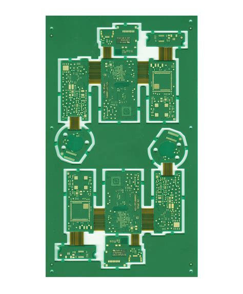
Printed Circuit Board (PCB) cloning, also known as reverse engineering, is a process used to recreate an existing PCB design for repair, improvement, or replication purposes. Double-sided PCB cloning involves copying both the top and bottom layers of a PCB, which requires precise techniques to ensure accuracy. This article outlines the essential operational steps for successfully cloning a double-sided PCB.
1. Preparation and Data Collection
Before starting the cloning process, gather the necessary tools and information:
Tools Required:
- High-resolution scanner or camera
- PCB design software (e.g., Altium Designer, KiCad, Eagle)
- Soldering iron and desoldering tools
- Multimeter for continuity testing
- Magnifying glass or microscope for inspection
Information Needed:
- Original PCB specifications (dimensions, layer count, material)
- Component list (resistors, capacitors, ICs, etc.)
- Schematic diagram (if available)
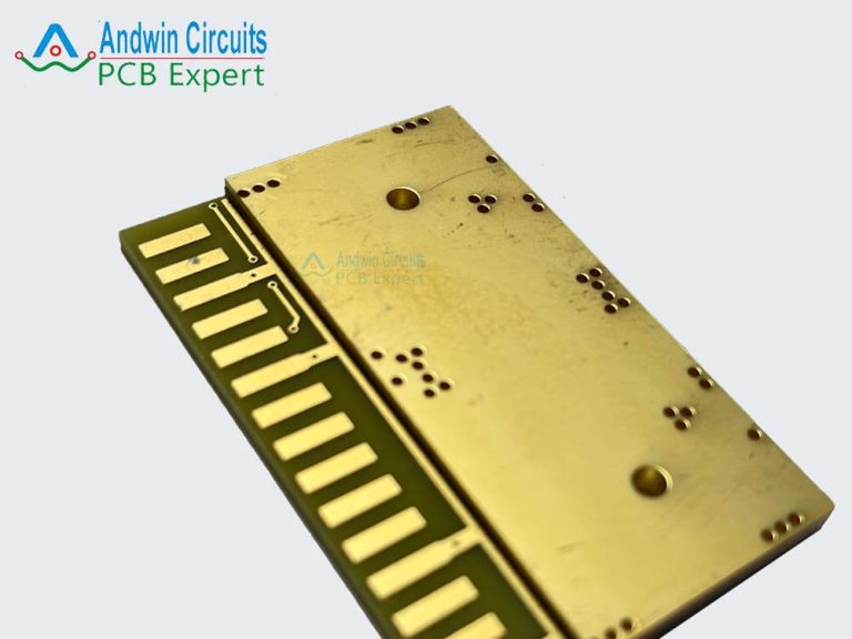
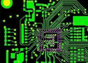
2. PCB Scanning and Image Processing
Since double-sided PCBs have conductive traces on both sides, high-quality scans are crucial.
Step-by-Step Process:
- Scan Both Sides:
- Use a high-resolution scanner (600 DPI or higher) to capture clear images of the top and bottom layers.
- Ensure proper lighting to avoid shadows or reflections.
- Image Alignment:
- Overlay the scanned images in PCB design software to ensure accurate layer matching.
- Adjust brightness and contrast to enhance trace visibility.
- Trace Extraction:
- Use software tools (e.g., Photoshop, GIMP) to clean up the images and remove noise.
- Convert the images into black-and-white for better trace recognition.
3. Schematic Reverse Engineering
Reconstructing the circuit schematic is essential for understanding the PCB’s functionality.
Key Steps:
- Component Identification:
- Label all components (ICs, resistors, capacitors, etc.) with their values and part numbers.
- Use a multimeter to check connections if markings are unclear.
- Trace Mapping:
- Manually or using software, map the connections between components.
- Verify continuity between traces to avoid errors.
- Schematic Drawing:
- Input the traced connections into PCB design software to generate a schematic.
- Cross-check with the original PCB to ensure accuracy.
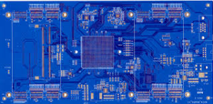
4. PCB Layout Design
After obtaining the schematic, the next step is recreating the PCB layout.
Process:
- Define Board Dimensions:
- Measure the original PCB and set the same dimensions in the design software.
- Component Placement:
- Position components as per the original PCB to maintain signal integrity.
- Ensure proper spacing to avoid interference.
- Trace Routing:
- Replicate the original trace paths, considering impedance and signal integrity.
- Use autorouting tools but manually verify critical traces.
- Via and Hole Placement:
- Mark via locations for inter-layer connections.
- Ensure drill holes match the original PCB.
5. Verification and Testing
Before manufacturing, the cloned design must be verified.
Testing Methods:
- Design Rule Check (DRC):
- Run DRC in the PCB software to detect errors like short circuits or missing connections.
- Netlist Comparison:
- Compare the cloned netlist with the original (if available) to ensure consistency.
- Prototype Testing:
- Manufacture a prototype and test functionality.
- Use an oscilloscope or logic analyzer to verify signal behavior.
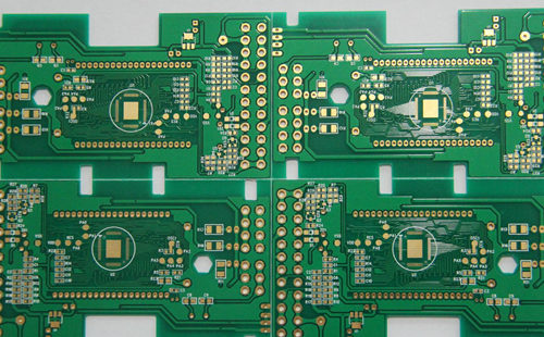
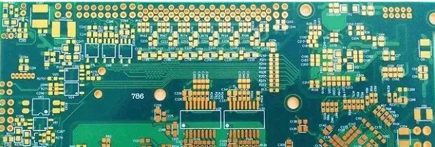
6. Manufacturing the Cloned PCB
Once verified, proceed with PCB fabrication.
Fabrication Steps:
- Gerber File Generation:
- Export Gerber files for both top and bottom layers, including drill files.
- PCB Fabrication:
- Send files to a PCB manufacturer or use DIY etching methods.
- Assembly:
- Solder components onto the new PCB.
- Perform functional testing to ensure it matches the original.
7. Quality Control and Final Checks
After assembly, conduct thorough testing.
Final Tests:
- Continuity Test: Ensure no open or short circuits.
- Power-On Test: Verify voltage levels and signal integrity.
- Functional Test: Check if the PCB performs as expected.
Conclusion
Double-sided PCB cloning requires meticulous attention to detail at every step—from scanning and schematic recreation to layout design and testing. By following these structured steps, engineers and hobbyists can accurately clone complex double-sided PCBs for repair, replication, or enhancement purposes. Proper verification ensures the cloned PCB functions identically to the original, making this technique invaluable in electronics reverse engineering.