PCB Electrical Design: Principles and Best Practices
Introduction to PCB Electrical Characteristics
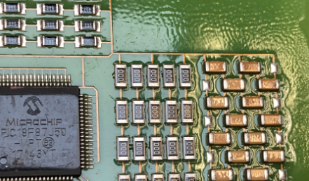
Printed Circuit Board (PCB) electrical design forms the foundation of all modern electronics. From simple consumer devices to complex aerospace systems, the electrical performance of a PCB directly determines the functionality, reliability, and efficiency of the entire electronic system. PCB electrical characteristics encompass all aspects of how electrical signals and power are distributed, transmitted, and managed across the board’s conductive pathways.
The electrical design of a PCB involves numerous critical considerations including impedance control, signal integrity, power distribution, electromagnetic compatibility, and thermal management. These factors interact in complex ways that require careful balancing during the design process. As electronic devices continue to shrink in size while increasing in capability and speed, the challenges of PCB electrical design become ever more demanding.
This article explores the fundamental principles of PCB electrical design, examining key concepts, common challenges, and best practices that engineers employ to create reliable, high-performance circuit boards. We will cover essential topics such as transmission line theory, power integrity, grounding strategies, and signal integrity considerations that form the core of effective PCB electrical engineering.
Transmission Line Theory and Impedance Control
Understanding Transmission Lines in PCBs
At high frequencies, PCB traces no longer behave as simple conductors but instead function as transmission lines. When signal wavelengths become comparable to trace lengths (typically at frequencies above 50-100 MHz), transmission line effects must be considered to maintain signal integrity. A transmission line consists of a signal conductor (trace) and its return path (usually a ground plane), with characteristic impedance determined by their geometry and the dielectric material between them.
The characteristic impedance (Z₀) of a PCB trace is given by:
Z₀ = √(L/C)
Where L is the distributed inductance per unit length and C is the distributed capacitance per unit length. For typical microstrip traces (on outer layers), impedance can be approximated by:
Z₀ ≈ [87/√(εᵣ + 1.41)] × ln[5.98h/(0.8w + t)]
Where:
- εᵣ is the dielectric constant of the substrate
- h is the height of the substrate
- w is the width of the trace
- t is the thickness of the trace
Impedance Matching Techniques
Impedance mismatches cause signal reflections that degrade signal quality. Common matching techniques include:
- Source Termination: Adding a series resistor at the driver equal to Z₀ minus the driver’s output impedance
- End Termination: Placing a parallel resistor at the receiver equal to Z₀
- Differential Pair Routing: Maintaining consistent spacing and length for differential signals
- Controlled Dielectrics: Using PCB materials with stable dielectric constants across frequency and temperature
Modern PCB design tools incorporate field solvers to calculate trace impedance based on stackup parameters, helping designers achieve precise impedance control.
Power Distribution Network (PDN) Design
The Importance of Power Integrity
A robust Power Distribution Network is crucial for stable operation of modern electronics. The PDN must provide clean, stable voltage to all components while minimizing voltage fluctuations (ripple and noise) that can cause timing errors or false switching. Key aspects of PDN design include:
- DC Voltage Drop: Ensuring adequate trace/w plane cross-sections to minimize IR drop
- AC Impedance: Maintaining low impedance across the frequency spectrum
- Decoupling Strategy: Proper use and placement of decoupling capacitors
- Plane Design: Effective use of power and ground planes
PDN Impedance Analysis
The target impedance (Ztarget) of a PDN can be calculated as:
Ztarget = (Vdd × Ripple%) / ΔI
Where:
- Vdd is the supply voltage
- Ripple% is the allowable voltage variation (typically 2-5%)
- ΔI is the maximum current transient
To achieve low impedance across a broad frequency range, designers employ a combination of:
- Bulk Capacitors (10-100μF): Handle low frequency demands
- Ceramic Capacitors (0.1-10μF): Address mid-range frequencies
- Small MLCCs (0.01-0.1μF): Handle high frequency needs
- Plane Capacitance: Exploit inherent capacitance between power-ground planes
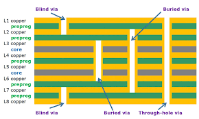
PCB Stackup for Power Integrity
An optimal stackup enhances PDN performance. Common approaches include:
- Adjacent Power-Ground Planes: Creates distributed capacitance
- Multiple Voltage Planes: For systems with several supply voltages
- Thin Dielectrics: Between power-ground pairs increases plane capacitance
- Strategic Via Placement: Minimizes loop inductance
Signal Integrity Considerations
Common Signal Integrity Issues
Signal integrity problems manifest in various ways:
- Reflections: Caused by impedance mismatches
- Crosstalk: Unwanted coupling between adjacent traces
- Ground Bounce: Voltage fluctuations in ground reference
- Simultaneous Switching Noise: Multiple outputs switching simultaneously
- Electromagnetic Interference (EMI): Radiated or conducted noise
Mitigation Strategies
- Proper Termination: As discussed in transmission line section
- Trace Spacing: Follow 3W rule (space ≥ 3× trace width) to minimize crosstalk
- Layer Stacking: Route sensitive signals between ground planes
- Differential Signaling: For high-speed interfaces
- Via Stitching: Around high-speed signals to provide continuous return paths
High-Speed Design Techniques
Modern high-speed designs (DDR memory, SerDes links, etc.) require additional considerations:
- Length Matching: Critical for parallel buses and differential pairs
- Via Optimization: Use back-drilling or microvias to minimize stubs
- Serpentine Routing: For precise length matching without sharp bends
- Reference Plane Continuity: Avoid splits under high-speed traces
Grounding Strategies
Ground System Architectures
The choice of grounding approach significantly impacts PCB performance:
- Single-Point Ground: All grounds connect at one point (good for low frequencies)
- Multi-Point Ground: Multiple connections to ground plane (better for high frequencies)
- Hybrid Ground: Combines aspects of both approaches
- Split Ground Planes: Used to isolate analog and digital sections
Ground Loop Prevention
Ground loops occur when multiple current return paths exist, potentially causing noise and interference. Prevention methods include:
- Proper Partitioning: Separate analog and digital grounds with a single connection point
- Star Grounding: Radiating all ground connections from a central point
- Avoiding Splits: In ground planes under high-frequency signals
EMI/EMC Considerations
Sources of EMI in PCBs
Electromagnetic interference arises from:
- High di/dt Circuits: Fast current changes create magnetic fields
- High dv/dt Signals: Fast voltage changes create electric fields
- Poor Return Paths: Forces currents to take unintended routes
- Slot Antennas: Created by gaps in planes or improper via fencing
EMI Reduction Techniques
- Proper Shielding: For sensitive or noisy circuits
- Filtering: On I/O lines and power inputs
- Edge Rate Control: Slowing unnecessary fast transitions
- Component Placement: Grouping related functions together
- Board Edge Considerations: Avoiding traces near board edges
Thermal Considerations in Electrical Design
Thermal-Electrical Interactions
Electrical performance is intimately tied to thermal conditions:
- Conductor Resistance: Increases with temperature (positive temperature coefficient)
- Dielectric Properties: Change with temperature
- Component Performance: Many parameters are temperature-dependent
- Reliability: Elevated temperatures accelerate failure mechanisms
Thermal Management Techniques
- Copper Thickness: Adequate for current carrying requirements
- Thermal Relief: For component pads connected to planes
- Via Arrays: To conduct heat between layers
- Copper Pour: For heat spreading
- Component Placement: Distributing heat sources evenly
Design for Manufacturing (DFM) Electrical Considerations
DFM Impacts on Electrical Performance
Manufacturing variations affect electrical characteristics:
- Etch Tolerance: Affects trace width and thus impedance
- Dielectric Thickness: Variations impact impedance and crosstalk
- Plating Uniformity: Affects via resistance and reliability
- Surface Finish: Impacts solderability and high-frequency losses
DFM Best Practices
- Conservative Rules: Allow margin for manufacturing variations
- Test Structures: Include test coupons for impedance verification
- Panelization Considerations: Account for routing near board edges
- Finish Selection: Choose appropriate surface finish for application
Future Trends in PCB Electrical Design
Emerging Challenges and Solutions
- Higher Frequencies: Millimeter-wave designs requiring advanced materials
- 3D Integration: Stacked dies and package-on-package technologies
- Advanced Materials: Low-loss dielectrics for high-speed applications
- AI-Assisted Design: Machine learning for optimization and troubleshooting
- Sustainable Electronics: Environmentally conscious material choices
Conclusion
PCB electrical design represents a complex interplay of physics, materials science, and engineering principles. As electronic systems continue to advance, the demands on PCB electrical performance grow increasingly stringent. Successful designs require careful consideration of transmission line effects, power distribution, signal integrity, grounding, and thermal management—all while accounting for manufacturing realities.
By understanding and applying the fundamental principles outlined in this article, electrical engineers can create PCBs that meet performance requirements while maintaining reliability and manufacturability. The field continues to evolve rapidly, with new materials, design techniques, and tools constantly emerging to address the challenges of next-generation electronics.
Ultimately, excellent PCB electrical design comes from balancing theoretical knowledge with practical experience, using advanced design tools while maintaining a solid grasp of first principles, and always verifying designs through careful simulation and prototyping. Those who master these skills will be well-equipped to tackle the electronic design challenges of today and tomorrow.