PCB Etching: A Comprehensive Guide to Printed Circuit Board Fabrication
Introduction
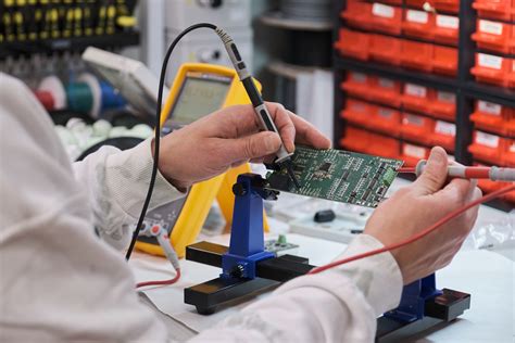
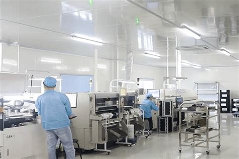
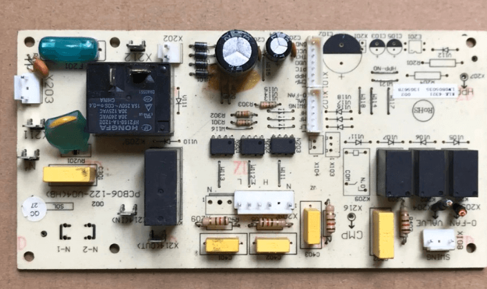
Printed Circuit Boards (PCBs) are the backbone of modern electronics, providing mechanical support and electrical connections for electronic components. One of the most critical steps in PCB manufacturing is etching, the process of removing unwanted copper from a PCB substrate to create conductive pathways. This article explores PCB etching in detail, covering different etching methods, chemicals used, process steps, advantages, challenges, and best practices.
1. Understanding PCB Etching
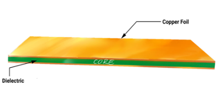
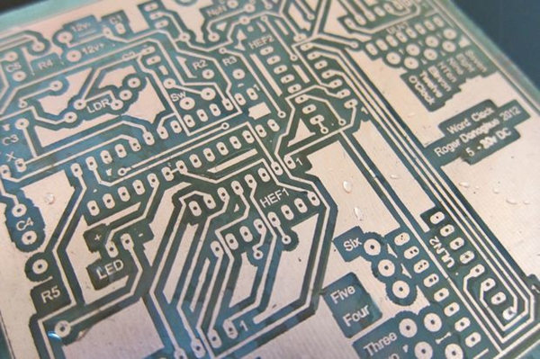
PCB etching is a subtractive manufacturing process where excess copper is chemically or mechanically removed from a PCB laminate, leaving behind the desired conductive traces. The process follows these general steps:
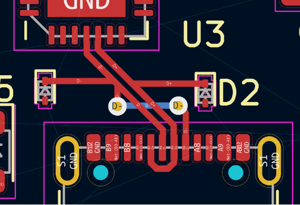
- PCB Design & Layout – A circuit design is created using CAD software and printed onto the board.
- Photoresist Application – A light-sensitive resist is applied to the copper-clad board.
- Exposure & Development – UV light transfers the circuit pattern onto the board, hardening the resist in desired areas.
- Etching – The exposed copper is dissolved using an etchant solution.
- Resist Removal – The remaining photoresist is stripped away, revealing the copper traces.
- Cleaning & Finishing – The board is cleaned, inspected, and coated with a protective layer.
2. Types of PCB Etching Methods
2.1 Chemical Etching
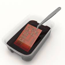
The most common method, chemical etching, uses acidic or alkaline solutions to dissolve unwanted copper.
Common Etchants:
- Ferric Chloride (FeCl₃) – A traditional etchant, effective but messy and corrosive.
- Ammonium Persulfate – Cleaner than ferric chloride but requires careful handling.
- Cupric Chloride (CuCl₂) – Used in industrial settings, regenerable for reuse.
- Hydrochloric Acid + Hydrogen Peroxide (HCl + H₂O₂) – Fast and effective but highly corrosive.
Process:
- The PCB is submerged in or sprayed with the etchant.
- The chemical reaction dissolves exposed copper.
- The board is rinsed to stop the etching process.
Advantages:
- High precision for fine traces.
- Suitable for mass production.
Disadvantages:
- Chemical waste disposal concerns.
- Requires safety precautions (gloves, ventilation).
2.2 Plasma Etching (Dry Etching)
Used in high-precision applications, plasma etching employs ionized gas to remove copper.
Process:
- The PCB is placed in a vacuum chamber.
- A reactive gas (e.g., CF₄, Cl₂) is ionized into plasma.
- The plasma reacts with copper, vaporizing it.
Advantages:
- No liquid chemicals required.
- High resolution for microelectronics.
Disadvantages:
- Expensive equipment.
- Slower than chemical etching.
2.3 Laser Etching
A modern technique where a high-power laser ablates unwanted copper.
Process:
- A laser beam scans the PCB surface.
- The copper is vaporized where the laser hits.
Advantages:
- No chemicals needed.
- High precision for prototyping.
Disadvantages:
- Slow for large-scale production.
- High initial cost.
3. Factors Affecting PCB Etching Quality
Several factors influence etching results:
3.1 Etchant Concentration & Temperature
- Higher temperatures speed up etching but may cause over-etching.
- Proper concentration ensures consistent copper removal.
3.2 Etching Time
- Too short: Incomplete copper removal.
- Too long: Undercutting of traces.
3.3 Agitation
- Stirring or spraying improves etch uniformity.
3.4 Copper Thickness
- Thicker copper requires longer etching times.
4. Challenges in PCB Etching
4.1 Over-Etching & Undercutting
Excessive etching can weaken traces, leading to breakage.
4.2 Incomplete Etching
Residual copper can cause short circuits.
4.3 Environmental Concerns
Chemical etchants require proper disposal to avoid pollution.
4.4 Safety Risks
Corrosive chemicals demand protective gear and ventilation.
5. Best Practices for Effective PCB Etching
- Use Fresh Etchant – Old or depleted solutions slow down the process.
- Monitor Temperature – Maintain optimal conditions (typically 40-50°C).
- Agitate the Solution – Ensures even copper removal.
- Inspect After Etching – Check for residual copper or defects.
- Dispose of Chemicals Safely – Follow environmental regulations.
6. Alternative PCB Fabrication Methods
While etching is widely used, other techniques include:
- Additive Processes – Electroless copper plating builds traces instead of removing copper.
- Milling – Mechanical removal of copper using CNC machines.
- Inkjet Printing – Conductive inks are printed directly onto substrates.
7. Future Trends in PCB Etching
- Eco-Friendly Etchants – Research into less toxic chemicals.
- Automated Etching Systems – Robotics for precision and efficiency.
- Laser Direct Structuring (LDS) – Combining lasers with plating for flexible PCBs.
Conclusion
PCB etching is a fundamental process in electronics manufacturing, enabling the creation of intricate circuit patterns. While chemical etching remains dominant, advancements in laser and plasma etching offer new possibilities. By understanding the different methods, challenges, and best practices, manufacturers can optimize etching for high-quality PCB production while minimizing environmental impact.
Would you like a more detailed section on any specific aspect, such as DIY etching or troubleshooting common issues?