PCB Fabrication and Assembly: A Comprehensive Overview
Introduction
Printed circuit boards (PCBs) are the foundation of modern electronic devices. Whether it is a simple household appliance or a complex computer system, PCBs play a vital role in it. This article will take a deep dive into the manufacturing and assembly process of PCBs, covering every step from design to final product.
I. Basics of PCBs
1.1 What is PCB?
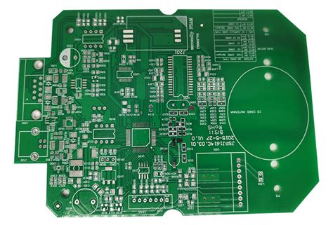
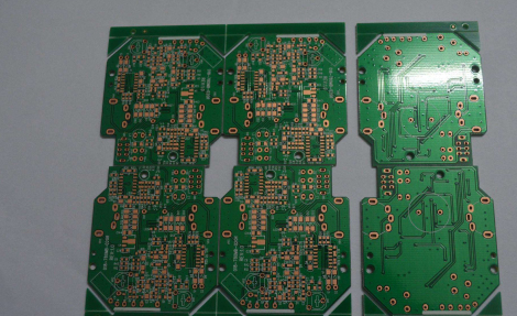
A printed circuit board (PCB) is a basic structure used to connect electronic components. It is usually made of an insulating material (such as FR-4) and the surface is covered with a conductive material (such as copper) to form a circuit. PCBs can be single-sided, multi-layered, or double-sided, depending on the complexity of the circuit and the required functions.
1.2 Types of PCBs
Single-sided PCB: Only one side has circuits, suitable for simple electronic products.
Double-sided PCB: Both sides have circuits, suitable for devices of medium complexity.
Multi-layer PCB: Contains three or more layers of circuits, suitable for high-complexity applications such as computers and communication equipment.
2.PCB Manufacturing Process
The manufacturing process of PCB can usually be divided into several main steps:
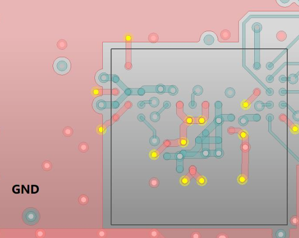
2.1 Design Phase
PCB manufacturing begins with the design phase. Designers use computer-aided design (CAD) software to create circuit diagrams and PCB layouts. The following factors need to be considered during the design process:
Circuit function: Ensure that the circuit can meet the design requirements.
Material selection: Select the appropriate substrate and conductive material.
Size and shape: Design the size and shape of the PCB according to the space limitations of the device.
2.2 Material preparation
The main materials of PCB include:
Substrate material: FR-4 (glass fiber reinforced epoxy resin) or other high-frequency materials are usually used.
Conductive material: Copper foil is usually used.
During the manufacturing process, the substrate material is cut into the required size and coated with a layer of photosensitive material for subsequent exposure and development processes.
2.3 Photolithography
Photolithography is a key step in PCB manufacturing. The process includes the following steps:
Coating photosensitive material: Evenly coat the photosensitive material on the surface of the substrate.
Exposure: Use an ultraviolet light source to project the designed circuit pattern onto a substrate coated with a photosensitive material.
Development: Remove the unexposed photosensitive material through a developer, leaving the circuit pattern.
2.4 Etching
Etching is the process of removing excess copper material to form a circuit. Common etching methods include:
Chemical etching: Use chemical solutions to remove unprotected copper.
Laser etching: Use lasers to remove the copper layer, suitable for PCBs with high precision requirements.
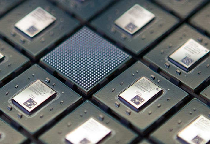
2.5 Electroplating
After etching, PCBs usually need to be electroplated to increase conductivity and improve durability. The electroplating process involves thickening the copper layer to ensure the reliability of the circuit.
2.6 Assembly preparation
After the PCB is manufactured, assembly preparation is carried out. This includes:
Drilling: Drill holes on the PCB according to design requirements to install electronic components.
Deburring: Clean the edges of the holes to ensure that the components can be installed smoothly.
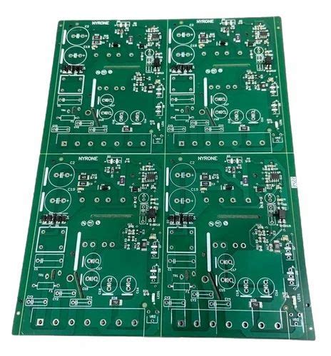
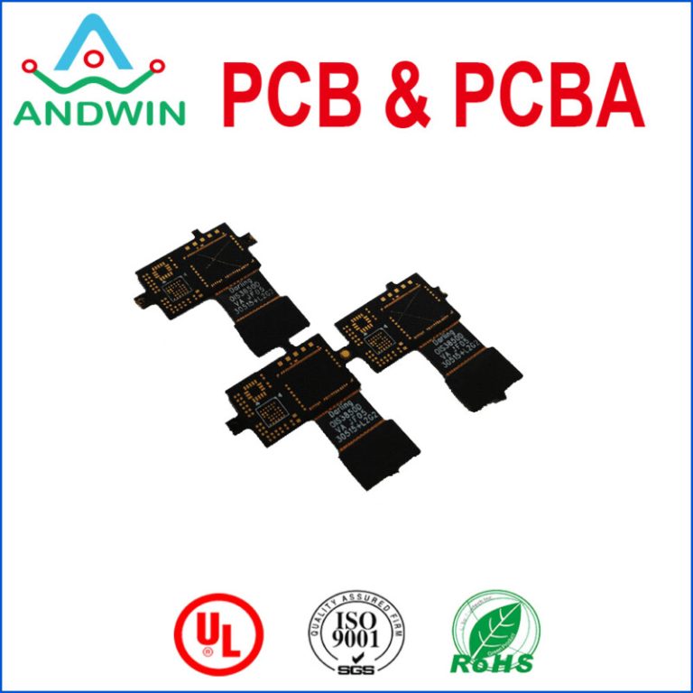
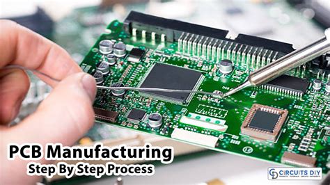
3.PCB assembly process
PCB assembly is the process of installing electronic components on the PCB. The assembly process usually includes the following steps:
3.1 Component Selection
Selecting the right electronic components is the first step in the assembly process. Common components include resistors, capacitors, integrated circuits (ICs), and connectors.
3.2 Printing Solder Paste
During the assembly process, solder paste needs to be printed on the pads of the PCB first. Solder paste is a viscous substance containing solder particles that is used to connect components and PCBs.
3.3 Component Placement
After the solder paste is printed, the electronic components are accurately placed on the pads of the PCB using an automatic placement machine. This step requires high precision to ensure the correct position of the components.
3.4 Reflow Soldering
After the components are placed, the PCB goes through a reflow soldering process. The process involves heating the PCB to a certain temperature so that the solder paste melts and forms a strong connection. Reflow soldering is usually performed in a dedicated reflow oven.
3.5 Inspection and Testing
After soldering is completed, the PCB needs to undergo rigorous inspection and testing to ensure that all connections are good and functioning properly. Common testing methods include:
Visual inspection: Check the solder joints and component positions.
Electrical testing: Test the electrical performance of the circuit to ensure that it meets the design requirements.
3.6 Packaging and delivery
After all tests are passed, the PCB will be packaged and ready for delivery to the customer. The packaging process includes cleaning the PCB, marking and packaging to ensure that it is not damaged during transportation.
4.Challenges of PCB manufacturing and assembly
Although PCB manufacturing and assembly technology has made significant progress, there are still some challenges:
4.1 Precision and complexity
As the complexity of electronic devices increases, the design and manufacture of PCBs have become more complex. Higher precision and smaller size are required, which puts higher requirements on manufacturing equipment and processes.
4.2 Cost control
The manufacturing and assembly costs of PCBs are affected by many factors, including material costs, equipment investment and labor costs. Enterprises need to strive to reduce costs while maintaining quality.
4.3 Environmental impact
The production process of PCBs may have an impact on the environment, including chemical waste and energy consumption. More and more companies are beginning to pay attention to sustainable development and seek environmentally friendly manufacturing methods.
5. Future Development Trends
With the continuous advancement of science and technology, the field of PCB manufacturing and assembly is also developing. The following trends may appear in the future:
5.1 Automation and intelligence
Automation equipment and intelligent manufacturing technology will further improve the production efficiency and quality of PCBs. The application of machine learning and artificial intelligence will make the production process more intelligent.
5.2 Application of new materials
The emergence of new materials will promote the development of PCB technology. For example, the application of flexible PCBs and high-frequency materials will provide more possibilities for the new generation of electronic products.
5.3 Environmentally friendly manufacturing
The increase in environmental awareness will prompt PCB manufacturers to adopt more environmentally friendly materials and processes to reduce the impact on the environment.
Conclusion
PCB manufacturing and assembly is a complex and delicate process involving multiple steps and technologies. With the continuous development of electronic products, PCB technology is also advancing. Understanding the manufacturing and assembly process of PCBs is crucial for professionals and enthusiasts engaged in the electronics industry. In the future, with the continuous advancement of technology, PCB manufacturing and assembly will usher in more opportunities and challenges.