PCB Fabrication and Assembly: Precision Techniques for Reliable Electronics
Key Takeaways
Modern PCB fabrication and assembly processes rely on precision engineering to ensure reliable electronics performance. Critical considerations include design optimization to minimize signal interference, material selection for thermal stability, and rigorous quality control protocols. Below is a comparative analysis of core aspects in PCBA workflows:
| Aspect | Fabrication Focus | Assembly Focus |
|---|---|---|
| Design Optimization | Layer alignment, trace routing | Component placement, soldering |
| Material Selection | Substrate dielectric properties | Solder alloy compatibility |
| Quality Control | Electrical testing | Automated optical inspection |
| Thermal Management | Copper weight distribution | Heat sink integration |
| Testing Protocols | Impedance matching checks | Functional validation |
Tip: Always prioritize Design for Manufacturing (DFM) checks during layout planning to avoid costly rework in PCB assembly stages.
The integration of automated optical inspection (AOI) systems in PCBA lines has reduced defect rates by up to 30%, while advanced solder paste printing techniques enhance joint reliability. For high-frequency applications, low-loss laminates like Rogers 4350B are critical to maintaining signal integrity. Transitioning between fabrication and assembly phases requires seamless data handoff, often managed through unified manufacturing execution systems (MES). By balancing thermal management strategies with material durability, manufacturers achieve compliance with IPC-A-610 standards for long-term operational stability.
PCB Fabrication and Assembly Techniques
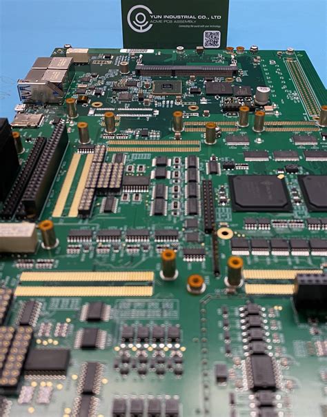
Modern PCB fabrication and PCB assembly processes rely on precision engineering to meet the escalating demands of electronic devices. The journey begins with translating design schematics into physical boards through photolithography, where copper-clad laminates are etched to create intricate circuit patterns. High-density interconnect (HDI) technologies enable multilayer stacking, critical for compact, high-performance electronics.
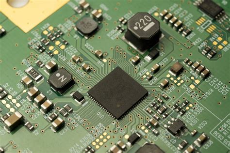
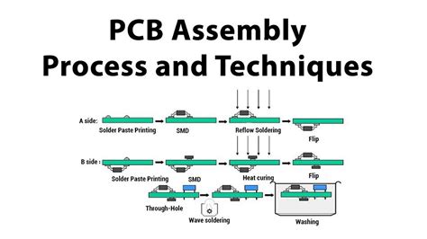
In PCBA (Printed Circuit Board Assembly), surface-mount technology (SMT) dominates, allowing rapid placement of microcomponents with sub-millimeter accuracy. Automated pick-and-place systems, paired with reflow soldering, ensure consistent electrical connections while minimizing human error. For specialized applications, mixed-technology assemblies combine through-hole components with SMT parts, balancing durability and miniaturization.
Material selection plays a pivotal role: flame-retardant substrates (FR-4) remain standard, but advanced applications demand polyimide flex circuits or ceramic-filled laminates for thermal stability. Post-assembly, automated optical inspection (AOI) and X-ray testing validate solder joint integrity, while in-circuit testing (ICT) confirms functional performance.
To maintain alignment with evolving industry standards, manufacturers increasingly adopt Industry 4.0 practices, integrating real-time analytics and machine learning to optimize yield rates. These techniques collectively ensure that PCB fabrication and assembly processes deliver robust, reliable circuitry, laying the foundation for next-generation electronics.
Optimizing PCB Layout Design Efficiency
Effective PCB assembly begins with intelligent layout design that balances electrical performance and manufacturing feasibility. Engineers achieve optimal efficiency by strategically positioning high-speed components to minimize signal interference while maintaining adequate clearance for PCBA processes. Automated routing tools now incorporate design rule checks (DRCs) to prevent common errors like trace congestion or insufficient thermal relief, reducing prototyping iterations by up to 40%.
A critical consideration involves aligning layer stack-ups with impedance control requirements, particularly for mixed-signal boards. For instance, separating analog and digital grounds early in the layout phase prevents noise coupling during PCB assembly. Additionally, adopting modular design principles allows reusable circuit blocks, accelerating development cycles for complex PCBA projects.
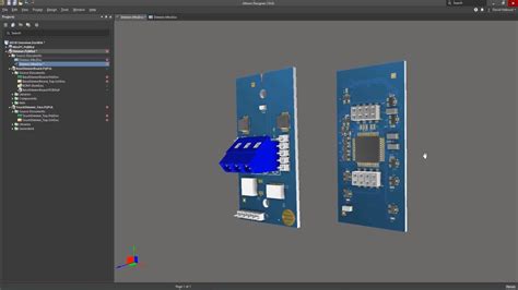
Transitioning to advanced CAD software with 3D visualization capabilities further enhances precision, enabling designers to simulate thermal dissipation paths and mechanical fitment before production. This proactive approach not only streamlines fabrication but also ensures compatibility with automated pick-and-place systems, a cornerstone of modern PCB assembly workflows. By integrating these strategies, manufacturers achieve faster time-to-market while maintaining the rigorous quality standards demanded by industries such as aerospace and medical electronics.
Selecting Materials for Durable PCBs
Material selection forms the cornerstone of creating durable PCBs capable of withstanding operational stresses. When designing boards for longevity, engineers prioritize thermal stability, mechanical strength, and chemical resistance in substrate materials. Common choices include FR-4 epoxy laminates for cost-effective applications, polyimide for flexible circuits, and ceramic-filled substrates for high-frequency or high-temperature environments. Critical considerations extend to copper weight—thicker layers enhance current-carrying capacity—and surface finishes like HASL (Hot Air Solder Leveling) or ENIG (Electroless Nickel Immersion Gold) to prevent oxidation and ensure reliable solder joints during PCB assembly.
For PCBA (Printed Circuit Board Assembly) processes, adhesives and solder pastes must align with the base material’s thermal expansion coefficient to avoid delamination under thermal cycling. Harsh-environment applications may require specialized coatings such as conformal coatings or potting compounds to shield against moisture and contaminants. This becomes particularly important in automotive or aerospace systems, where vibration resistance and long-term reliability are non-negotiable.
Equally crucial is verifying material compatibility with lead-free soldering processes, a standard in modern electronics manufacturing. Manufacturers must also weigh cost against performance, balancing advanced materials like high-Tg laminates against budget constraints without compromising durability. Environmental factors, including RoHS compliance, further guide decisions to meet global regulatory standards.
Quality Control in Electronics Manufacturing
Effective PCB assembly processes rely on rigorous quality control protocols to ensure the reliability of finished PCBA (Printed Circuit Board Assembly) products. Modern electronics manufacturing integrates automated inspection systems, such as Automated Optical Inspection (AOI) and X-ray imaging, to detect soldering defects, component misalignment, or micro-cracks in multilayer boards. These tools are critical for identifying issues early, reducing rework costs, and maintaining compliance with industry standards like IPC-A-610.
Material verification forms another cornerstone of quality assurance. Manufacturers cross-check substrate laminates, solder masks, and conductive inks against design specifications to prevent thermal degradation or electrical failures. For PCBA workflows, in-circuit testing (ICT) validates electrical connectivity, while functional testing simulates real-world operating conditions to assess performance under stress.
Rigorous process controls further minimize variability. Temperature profiling in reflow ovens ensures consistent solder joint formation, while traceability systems track each batch through the PCB fabrication and assembly lifecycle. By combining advanced inspection technologies with standardized protocols, manufacturers achieve near-zero defect rates, delivering electronics that meet both durability and precision requirements for applications ranging from consumer devices to aerospace systems.
Advanced PCB Manufacturing Process Insights
Modern PCB fabrication has evolved into a highly coordinated sequence of precision-driven stages, combining automated systems with rigorous process controls. At the core of PCB assembly (PCBA), manufacturers employ surface-mount technology (SMT) to place microcomponents with sub-millimeter accuracy, while laser-direct imaging ensures trace alignment tolerances below 5µm. Advanced material science plays a pivotal role, with high-performance substrates like high-Tg laminates and low-loss dielectrics mitigating signal degradation in high-frequency applications.
Critical to reliable electronics production is the integration of real-time monitoring during PCBA stages, where automated optical inspection (AOI) and X-ray systems detect solder joint defects or component misalignments at rates exceeding 10,000 inspections per hour. For multilayer boards, sequential lamination cycles paired with controlled impedance testing maintain signal integrity across complex stackups. Transitioning from fabrication to PCB assembly, manufacturers implement nitrogen-reflow soldering to minimize oxidation, achieving void rates under 2% in BGA connections.
To align with evolving industry demands, adaptive manufacturing workflows now incorporate design-for-manufacturability (DFM) checks during PCB fabrication, reducing post-production revisions by 40–60%. This synergy between PCBA precision and process innovation ensures compliance with IPC-A-610 and MIL-PRF-31032 standards, while enabling scalable solutions for IoT and automotive-grade electronics. As thermal management grows critical, embedded copper coin technology and selective gold plating are increasingly adopted to enhance durability under extreme operating conditions.
Precision Assembly for Reliable Circuitry
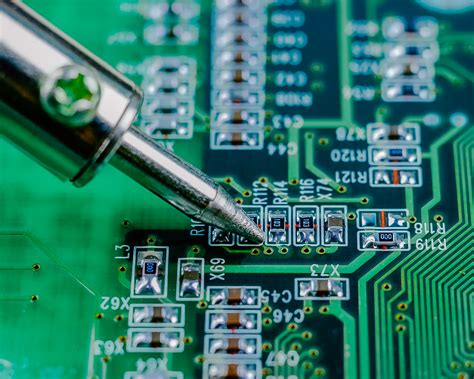
Modern PCB assembly processes demand meticulous attention to detail to ensure consistent performance in electronic systems. At the core of PCBA (printed circuit board assembly), automated pick-and-place systems position surface-mount devices (SMDs) with micron-level accuracy, minimizing human error and enhancing repeatability. Critical steps such as solder paste application and reflow profiling require precise temperature control to prevent defects like tombstoning or cold joints. For mixed-technology boards, selective soldering techniques combine wave soldering for through-hole components with laser-assisted reflow for delicate micro-BGA packages, balancing efficiency and reliability.
Advanced PCBA workflows integrate inline optical inspection (AOI) systems to detect misalignments or solder anomalies in real time, ensuring compliance with IPC-A-610 standards. Environmental controls, including cleanroom conditions and humidity stabilization, further safeguard sensitive components during assembly. The growing adoption of 3D SPI (solder paste inspection) tools enables pre-reflow defect detection, reducing rework costs and improving yield rates. By aligning PCB assembly protocols with design-for-manufacturability (DFM) principles, engineers achieve optimal signal integrity and thermal management—key factors in high-frequency or power-dense applications. These precision-driven methodologies not only extend product lifespans but also reinforce the foundation for scalable, high-reliability electronics manufacturing.
Testing Protocols for Enhanced PCB Reliability
Rigorous testing protocols form the backbone of dependable PCB assembly processes, ensuring end products meet mission-critical performance standards. Modern PCBA workflows integrate automated optical inspection (AOI) to detect soldering defects, component misalignment, or trace irregularities at micron-level precision. Advanced techniques like in-circuit testing (ICT) validate electrical continuity, while functional testing simulates real-world operating conditions to assess signal integrity and power distribution.
Environmental stress screening (ESS) further elevates reliability by exposing assembled boards to controlled thermal cycling, humidity extremes, and vibration tests—identifying latent failures before deployment. For high-frequency applications, impedance testing and time-domain reflectometry (TDR) ensure signal paths maintain design specifications.
Quality-centric PCB fabrication and assembly teams leverage boundary-scan methodologies to diagnose complex multilayer interconnects, complemented by X-ray inspection for hidden solder joint analysis. These protocols not only align with IPC-A-610 and J-STD-001 standards but also adapt to emerging challenges like miniaturized components and high-density interconnects (HDIs). By embedding proactive testing at every PCBA stage, manufacturers mitigate field failures and extend product lifespans across industrial, automotive, and aerospace applications.
Thermal Management in PCB Design Solutions
Effective thermal management remains a critical consideration in PCB assembly, where improper heat dissipation can compromise circuit integrity and component longevity. Modern PCBA processes integrate advanced techniques such as thermal vias, copper pours, and strategically placed heat sinks to channel excess energy away from sensitive components. Designers optimize layouts by analyzing thermal hotspots through simulation tools, ensuring even distribution across multilayer boards. Material selection plays a dual role here: high-glass transition temperature (Tg) substrates and metal-core laminates enhance heat resistance, while solder mask choices influence surface emissivity. During PCB fabrication, controlled impedance traces and optimized copper weights further mitigate thermal stress. Rigorous post-assembly testing, including infrared thermography, validates performance under operational loads, aligning with industry standards for reliability in high-power applications like automotive or IoT devices. By harmonizing design precision with material science, engineers achieve thermally stable solutions that extend product lifecycles without sacrificing functionality.
Conclusion
The evolution of PCB fabrication and assembly underscores the critical balance between precision engineering and scalable manufacturing practices. As industries demand higher reliability in electronic systems, integrating design-for-manufacturability principles with PCBA workflows becomes indispensable. Modern PCB assembly processes leverage automated placement systems and reflow soldering techniques to ensure consistent component alignment and electrical integrity, particularly in high-density layouts.
Rigorous quality assurance protocols, including automated optical inspection (AOI) and functional testing, remain central to identifying defects in PCBA outputs before deployment. Equally vital is the alignment of material choices with operational environments—whether selecting high-temperature laminates or low-loss dielectrics—to enhance thermal stability and signal performance.
Ultimately, the success of PCB fabrication and assembly hinges on harmonizing advanced manufacturing technologies with meticulous oversight at every stage. As industries push toward miniaturization and IoT-driven applications, adopting data-driven process optimization will continue to define competitiveness in electronics manufacturing. By prioritizing both innovation and traceability, stakeholders can deliver circuitry that meets evolving reliability benchmarks while minimizing lifecycle costs.
Frequently Asked Questions
What distinguishes PCB assembly from PCBA?
PCB assembly refers to the process of populating a bare circuit board with components, while PCBA (Printed Circuit Board Assembly) denotes the completed, functional board after all parts are soldered and tested. Both terms are often used interchangeably, but PCBA emphasizes the finalized product ready for integration into electronic devices.
How does material selection impact PCB assembly reliability?
Material choices, such as high-temperature substrates or low-loss dielectrics, directly affect thermal stability and signal integrity. For instance, FR-4 epoxy is common for standard applications, while polyimide is preferred for flexible PCBA designs requiring durability under stress.
What quality control measures ensure defect-free PCB assembly?
Automated Optical Inspection (AOI) and X-ray testing are critical for identifying soldering defects or misaligned components. Additionally, In-Circuit Testing (ICT) validates electrical performance, ensuring every PCBA meets predefined functional benchmarks before shipment.
Why is thermal management vital in PCBA design?
Excessive heat degrades component lifespan and performance. Techniques like thermal vias, copper pours, and heat sinks dissipate energy efficiently, maintaining optimal operating temperatures for high-power PCB assembly configurations.
Can design errors be corrected during PCB assembly?
Minor issues, such as incorrect resistor values, can be reworked manually. However, major layout flaws often necessitate redesigning the board, underscoring the importance of Design for Manufacturability (DFM) checks before initiating PCBA production.
Optimize Your Next PCB Assembly Project Today
For expert guidance on optimizing your PCB assembly processes, please click here to explore tailored solutions that ensure precision and reliability in every PCBA delivery.