PCB Fabrication Essentials: Processes and Innovations
Key Takeaways
Understanding PCB manufacturing fundamentals helps you navigate complex production decisions. Modern PCB manufacturing companies prioritize material innovation and precision engineering to meet evolving demands, balancing PCB manufacturing cost with performance requirements. When evaluating your PCB manufacturing business, consider how advanced techniques like laser direct imaging (LDI) and automated optical inspection (AOI) enhance yield rates while reducing errors.
Key cost drivers include layer count, substrate materials, and surface finishes—each impacting both functionality and budget. For instance, opting for high-frequency laminates might raise initial expenses but improve signal integrity in advanced applications. Meanwhile, sustainable practices like lead-free finishes and waste-reduction protocols are reshaping industry standards, aligning profitability with environmental responsibility.
Stay informed about emerging technologies such as additive manufacturing and AI-driven process optimization, which enable faster prototyping and smarter resource allocation. By mastering these dynamics, you’ll better assess suppliers, streamline workflows, and maintain competitiveness in a sector where precision and adaptability define success.
PCB Fabrication Core Principles Explained
Understanding the core principles of PCB manufacturing begins with recognizing how design accuracy intersects with material science. At its foundation, every circuit board relies on precise layering of conductive and insulating materials, a process refined by PCB manufacturing companies to balance performance and PCB manufacturing cost. You’ll find that modern fabrication prioritizes design-for-manufacturability (DFM), ensuring layouts minimize waste and maximize yield.
Key steps like photolithography, etching, and lamination demand meticulous control, where even minor deviations can escalate PCB manufacturing business expenses. For example, improper alignment during etching risks short circuits, while suboptimal material choices—such as high-frequency laminates for 5G devices—directly impact thermal and electrical performance. To stay competitive, leading manufacturers adopt advanced automation to standardize processes, reducing human error and variability.
Critical to these principles is the interplay between thermal management and signal integrity. Innovations like embedded passives or high-density interconnect (HDI) designs push boundaries but require tighter tolerances. When collaborating with PCB manufacturing companies, you’ll notice how cost-efficiency hinges on balancing advanced techniques with scalable production frameworks—ensuring quality without compromising affordability. By mastering these fundamentals, the industry continues to evolve, addressing both technical challenges and market demands.
Cutting-Edge Circuit Board Material Innovations
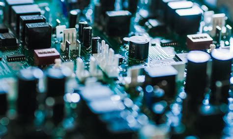
Modern pcb manufacturing relies heavily on breakthroughs in substrate materials to meet evolving performance demands. As devices shrink and frequencies rise, traditional FR-4 laminates are being replaced by advanced composites like Rogers 4000 series or PTFE-based dielectrics. These materials offer superior signal integrity for high-speed applications while minimizing pcb manufacturing cost through improved thermal stability and reduced layer counts.
Leading pcb manufacturing companies now integrate flexible polyimide substrates for wearable tech and foldable electronics, enabling thinner, lighter designs without sacrificing durability. For harsh environments, ceramic-filled polymers and metal-core boards enhance heat dissipation, extending component lifespans—a critical factor for automotive and aerospace applications.
| Material Type | Key Properties | Primary Applications |
|---|---|---|
| High-Frequency Laminates | Low dielectric loss, <0.002 Dk | 5G infrastructure, radar systems |
| Flexible Substrates | Bend radius <1mm, <0.1mm thickness | Medical sensors, foldable displays |
| Thermal Management Boards | Thermal conductivity >5 W/mK | EV power modules, LED lighting |
Sustainability is reshaping the pcb manufacturing business, with bio-based resins and halogen-free laminates gaining traction. While these alternatives may initially increase pcb manufacturing cost, they align with global regulations and reduce long-term environmental liabilities. By balancing performance metrics with ecological responsibility, manufacturers can future-proof their designs while addressing tighter industry standards.
Precision Manufacturing Techniques for PCBs
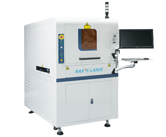
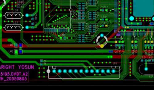
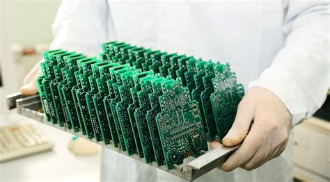
Achieving precision manufacturing in PCB manufacturing requires balancing technical expertise with advanced equipment. Modern PCB manufacturing companies employ laser direct imaging (LDI) systems to create circuit patterns with micron-level accuracy, eliminating photomasks and reducing alignment errors. Automated optical inspection (AOI) tools then scan boards in real time, flagging defects like micro-shorts or incomplete etches before they escalate PCB manufacturing costs. For high-density designs, sequential lamination ensures layer alignment within ±25µm, while controlled impedance routing maintains signal integrity in high-frequency applications.
To optimize PCB manufacturing business workflows, firms integrate Industry 4.0 practices—IoT-enabled machinery monitors production variables like temperature and pressure, adjusting parameters autonomously for consistent output. Advanced plating techniques, such as pulse electroplating, enhance copper deposition uniformity, critical for fine-pitch components. These innovations not only improve yield rates but also enable tighter tolerances demanded by wearables and aerospace electronics. By adopting such techniques, you ensure your designs transition from prototype to mass production without compromising performance or reliability.
Evolution of PCB Production Technologies
The journey of PCB manufacturing has transformed radically since its mid-20th-century origins. Early methods relied on manual etching and rudimentary drilling, limiting design complexity and scalability. Today, advancements like laser direct imaging (LDI) and automated optical inspection (AOI) enable PCB manufacturing companies to produce multilayer boards with micron-level precision while reducing PCB manufacturing cost through streamlined workflows.
Modern techniques such as additive manufacturing and embedded component integration are redefining design boundaries, allowing for lighter, faster, and more energy-efficient electronics. Automation plays a pivotal role here—robotic assembly lines and AI-driven quality checks minimize human error, ensuring consistency even in high-volume production.
"Adopting flexible manufacturing systems isn’t just about speed; it’s about future-proofing your PCB manufacturing business against shifting market demands."
Environmental regulations have also driven innovation. Lead-free soldering and halogen-free substrates now dominate the industry, balancing performance with sustainability. As you evaluate production partners, prioritize those leveraging advanced data analytics to optimize material usage and waste reduction—critical factors for both cost efficiency and eco-compliance.
From rigid single-layer boards to stretchable circuits for wearables, the evolution of PCB manufacturing reflects the relentless push toward miniaturization and functionality. Staying ahead means embracing these technological leaps while maintaining rigorous quality standards at every stage.
Advanced Process Optimization Strategies
When optimizing PCB manufacturing processes, you need to balance precision with efficiency. Leading PCB manufacturing companies now deploy real-time monitoring systems to track parameters like etching depth and copper plating uniformity, reducing defects by up to 30%. By integrating machine learning algorithms, these systems predict tool wear and adjust workflows dynamically, ensuring consistent quality while minimizing PCB manufacturing cost.
Material utilization is another critical focus. Advanced nesting software arranges circuit patterns to maximize panel usage, cutting waste by 15–20%. This not only lowers raw material expenses but also aligns with sustainability goals—a growing priority for the PCB manufacturing business. For high-density designs, laser direct imaging (LDI) replaces traditional photomasks, slashing alignment errors and accelerating prototyping cycles.
Thermal management strategies also play a pivotal role. Controlled impedance drilling and optimized solder mask applications prevent warping in multilayer boards, even under high-temperature reflow. By adopting these innovations, manufacturers can scale production without compromising reliability—a key advantage in competitive markets.
Finally, collaboration between design and fabrication teams ensures Design for Manufacturing (DFM) principles are embedded early. This reduces iterative revisions, streamlines timelines, and ultimately sharpens your edge in delivering cutting-edge electronics.
Sustainable Practices in PCB Fabrication
As environmental concerns reshape industries, PCB manufacturing companies are adopting sustainable methods to balance efficiency with ecological responsibility. You’ll find modern facilities prioritizing lead-free soldering and halogen-free laminates, reducing hazardous substances while maintaining performance. Innovations like water-based cleaning systems and recycling programs for copper clads and solvents are cutting waste in PCB manufacturing, aligning with global circular economy goals.
When evaluating PCB manufacturing cost, sustainable practices often yield long-term savings. Energy-efficient laser drilling and direct imaging systems lower power consumption, while optimized panel utilization reduces material waste. Some companies even integrate renewable energy sources, slashing operational carbon footprints. For your PCB manufacturing business, adopting these methods not only meets regulatory standards but also appeals to eco-conscious clients.
Transitioning to greener processes doesn’t compromise precision. Advanced renewable substrate materials like biodegradable polymers or recycled fiberglass are gaining traction, offering durability with fewer environmental impacts. By partnering with certified PCB manufacturing providers, you ensure compliance with sustainability benchmarks like ISO 14001 or UL ECOLOGO—critical for maintaining competitiveness in a market increasingly driven by green credentials.
These shifts highlight how sustainability is no longer optional but a strategic advantage in PCB manufacturing, merging technical excellence with planetary stewardship.
Emerging Technologies Shaping PCB Manufacturing
As PCB manufacturing evolves, cutting-edge innovations are redefining how precision, speed, and sustainability intersect in production. Advanced automation systems now integrate AI-driven defect detection, enabling PCB manufacturing companies to reduce errors by over 30% while accelerating throughput. For instance, machine learning algorithms analyze micro-imperfections in real time, ensuring higher yield rates without compromising PCB manufacturing cost efficiency.
Another breakthrough lies in additive manufacturing techniques like inkjet-printed circuitry, which eliminates traditional etching steps. This not only slashes material waste but also supports flexible designs for wearables and IoT devices—critical for staying competitive in the PCB manufacturing business. Meanwhile, embedded component technology (ECT) allows passive components to be layered directly into substrates, shrinking board sizes and enhancing performance.
Sustainability is also driving innovation. Companies are adopting bio-based substrates and halogen-free laminates to meet eco-regulations, reducing reliance on toxic chemicals. Additionally, IoT-enabled smart factories leverage data analytics to optimize energy consumption, further trimming operational costs.
By embracing these advancements, you can future-proof your operations while balancing PCB manufacturing cost constraints with rising demand for miniaturized, high-performance boards. The key lies in strategically integrating automation, novel materials, and eco-conscious practices to stay ahead in this rapidly transforming industry.
Quality Control in Modern Circuit Board Production
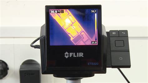
Maintaining rigorous quality control standards is non-negotiable in high-volume PCB manufacturing, where even minor defects can lead to catastrophic failures in electronic devices. Leading PCB manufacturing companies now deploy automated optical inspection (AOI) systems to scan for flaws like misaligned traces or solder bridging, ensuring precision at micron-level tolerances. Advanced X-ray imaging further verifies internal layer alignment in multilayer boards, while thermal stress testing simulates real-world operating conditions to assess durability.
To balance PCB manufacturing cost and reliability, statistical process control (SPC) tools track production metrics in real time, enabling data-driven adjustments to etching, drilling, or plating stages. Environmental controls—such as humidity-regulated cleanrooms—minimize contamination risks that could compromise final product performance. For businesses scaling a PCB manufacturing business, certifications like ISO 9001 and IPC Class 3 compliance have become critical differentiators, signaling adherence to global quality benchmarks.
Innovations like AI-powered defect prediction are reshaping workflows, reducing waste by identifying potential issues before they escalate. By integrating these strategies, manufacturers ensure every board meets exacting standards, whether producing prototypes or mass-market solutions.
Conclusion
As you navigate the complexities of PCB manufacturing, it becomes clear that balancing technical precision with economic viability defines success in this field. Leading PCB manufacturing companies now prioritize innovations that reduce PCB manufacturing cost while enhancing performance—whether through advanced materials, automated workflows, or waste-reduction strategies. When planning your PCB manufacturing business, consider how emerging technologies like additive printing or AI-driven quality control can future-proof operations against shifting market demands.
The evolution from traditional etching to laser-direct imaging exemplifies how process optimization reshapes production timelines and accuracy. Equally critical is adopting sustainable practices, such as recyclable substrates or energy-efficient facilities, to align with global environmental standards. By integrating these advancements, you position your projects at the intersection of reliability and scalability, ensuring that every circuit board meets both technical specifications and cost-efficiency targets.
Ultimately, the convergence of precision engineering, material science, and smart manufacturing continues to redefine what’s possible in electronics development—making this an era of unprecedented opportunity for those ready to innovate.
FAQs
How does PCB fabrication differ from PCB manufacturing?
While fabrication refers to creating the bare board through etching and layering, PCB manufacturing encompasses the entire process—from design and material selection to assembly and testing. Understanding this distinction helps when collaborating with PCB manufacturing companies.
What factors most impact PCB manufacturing cost?
Key drivers include board complexity, material choices (like high-frequency laminates), and order volume. Advanced features such as microvias or HDI designs typically increase PCB manufacturing cost, but bulk orders often reduce per-unit expenses.
Can small businesses compete in the PCB manufacturing business?
Yes, niche specialization—such as prototyping or flexible PCBs—allows smaller firms to thrive. Many PCB manufacturing companies now leverage automated tools to offer cost-effective, low-volume production tailored to startups.
How have recent innovations improved PCB manufacturing reliability?
Advances like laser direct imaging and automated optical inspection (AOI) minimize human error. Modern PCB manufacturing also integrates AI-driven analytics to predict and prevent defects during production.
What certifications should I prioritize when selecting a PCB partner?
Look for ISO 9001 (quality management) and UL certification. For specialized applications, IPC Class 3 or AS9100 (aerospace) compliance ensures adherence to rigorous PCB manufacturing standards.
Ready to Start Your PCB Project?
Streamline your next electronics design with precision-engineered solutions. Please click here to connect with industry-leading experts in PCB manufacturing and optimize your production workflow today.