PCB Fanout Techniques: Essential Tips for Efficient Design
Introduction
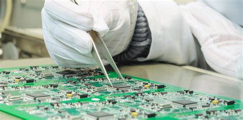
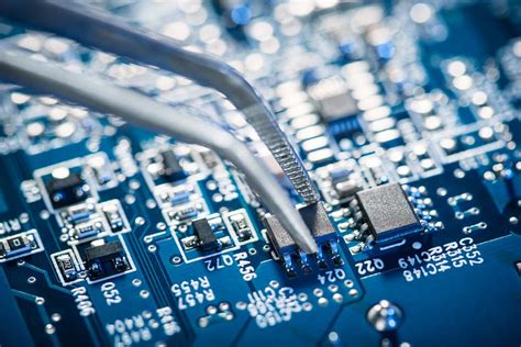
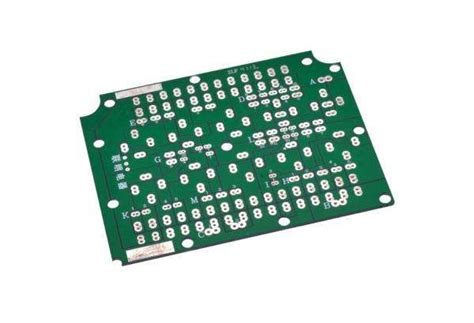
Printed Circuit Board (PCB) design is a complex process that requires careful planning, especially when dealing with high-density components and high-speed signals. One critical aspect of PCB layout is fanout—the process of routing traces from component pins to vias or other connections. Proper fanout techniques ensure signal integrity, manufacturability, and thermal management.
This article explores key PCB fanout techniques, best practices, and common mistakes to avoid, helping designers optimize their layouts for performance and reliability.
1. Understanding PCB Fanout
Fanout refers to the method of connecting component pins (such as those on BGAs, QFNs, or fine-pitch ICs) to the rest of the PCB through vias and traces. A well-executed fanout ensures:
- Signal Integrity: Minimizes crosstalk and impedance mismatches.
- Manufacturability: Ensures the design can be fabricated without defects.
- Thermal Management: Helps dissipate heat efficiently.
- Routing Efficiency: Simplifies further trace routing.
2. Key Fanout Techniques
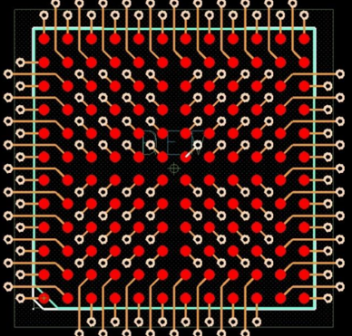
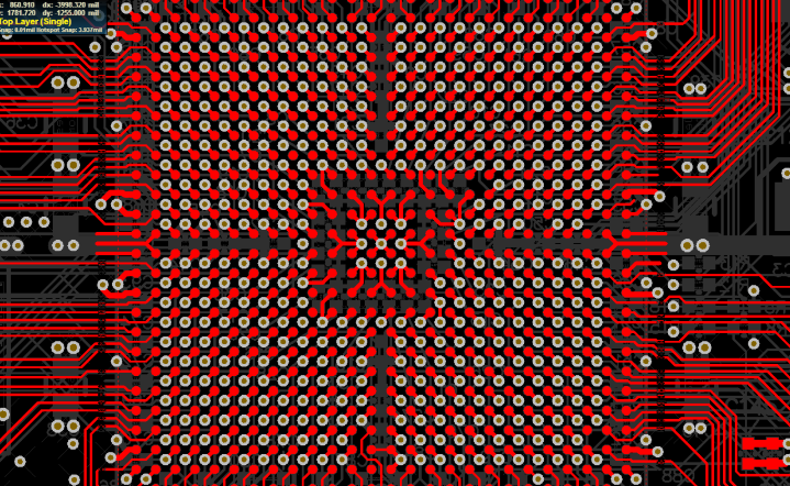
2.1. BGA Fanout Strategies
Ball Grid Arrays (BGAs) are among the most challenging components for fanout due to their high pin density. Common techniques include:
A. Escape Routing
- Dog-Bone Fanout: Uses short traces from BGA pads to vias, resembling a dog-bone shape. This is ideal for standard BGAs.
- Via-in-Pad: Places vias directly under BGA pads, saving space but requiring specialized manufacturing (filled or plugged vias).
- Staggered Vias: Alternates via placement in diagonal patterns to maximize routing channels.
B. Layer Utilization
- Microvias: Uses smaller vias (e.g., 0.1mm) to escape tight BGA pitches.
- Buried/Blind Vias: Reduces layer count but increases cost. Useful for high-density designs.
2.2. QFN and LGA Fanout
Quad Flat No-Lead (QFN) and Land Grid Array (LGA) packages require careful fanout due to their exposed pads and tight pin spacing.
- Thermal Pad Connections: Use multiple vias under thermal pads for heat dissipation.
- Peripheral Trace Routing: Fan out traces from the sides, avoiding congestion.
2.3. High-Signal Fanout
For high-speed signals (e.g., DDR, PCIe, USB), fanout must minimize impedance discontinuities:
- Differential Pair Fanout: Keep pairs symmetrical with matched lengths.
- Controlled Impedance Routing: Use proper trace width and spacing based on dielectric properties.
- Minimize Stub Lengths: Shorten via stubs to reduce signal reflections.
3. Best Practices for Efficient Fanout
3.1. Optimize Via Placement
- Avoid Via Crowding: Space vias sufficiently to prevent PCB fabrication issues (e.g., drill breakage).
- Use Teardrops: Add teardrops at trace-via junctions to strengthen connections and reduce stress.
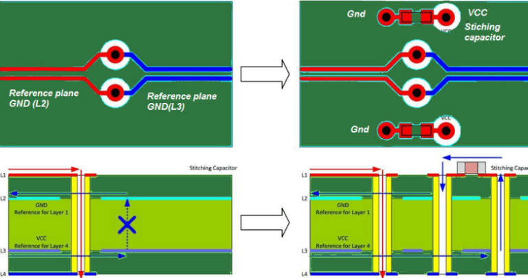
3.2. Layer Stackup Planning
- Dedicated Signal & Ground Layers: Helps maintain consistent impedance.
- Power Plane Considerations: Ensure power vias do not obstruct signal routing.
3.3. Automated vs. Manual Fanout
- Automated Tools: Many PCB design tools (Altium, Cadence, KiCad) offer auto-fanout features, but manual adjustments are often needed for optimization.
- Manual Tweaking: Adjust trace lengths, via placements, and escape routes for critical signals.
3.4. DFM (Design for Manufacturability) Checks
- Via Size & Aspect Ratio: Follow manufacturer guidelines (e.g., 8:1 aspect ratio for mechanical drills).
- Trace Width & Spacing: Ensure compliance with fabrication capabilities.
4. Common Fanout Mistakes & How to Avoid Them
| Mistake | Consequence | Solution |
|---|---|---|
| Insufficient Via Spacing | Drill breakage, short circuits | Follow manufacturer’s via spacing rules |
| Long Stub Lengths | Signal integrity degradation | Use back-drilling or blind vias |
| Poor Thermal Pad Fanout | Overheating issues | Add multiple thermal vias |
| Unbalanced Differential Pairs | Signal skew & EMI | Ensure symmetrical routing |
| Excessive Layer Changes | Increased cost & complexity | Optimize layer transitions |
5. Advanced Fanout Techniques
5.1. HDI (High-Density Interconnect) Fanout
- Laser Microvias: Allow finer pitch routing in compact designs.
- Stacked & Staggered Vias: Improve routing density in multilayer PCBs.
5.2. Flex & Rigid-Flex PCB Fanout
- Avoid Sharp Bends: Use curved traces to prevent cracking.
- Staggered Vias in Flex Areas: Reduces mechanical stress.
5.3. RF & Microwave Fanout
- Ground Via Fences: Shields high-frequency signals.
- Minimize Parasitics: Use short, direct traces with controlled impedance.
6. Conclusion
Effective PCB fanout is crucial for signal integrity, manufacturability, and thermal performance. By applying the right techniques—such as optimized via placement, layer planning, and adherence to DFM rules—designers can achieve efficient and reliable PCB layouts.
Whether working with BGAs, high-speed signals, or HDI designs, mastering fanout strategies will significantly improve PCB performance and reduce production issues. Always validate designs through simulation and prototyping before finalizing the layout.