PCB Fault Repair:A Comprehensive Guide
Printed Circuit Boards (PCBs) are the backbone of modern electronics, found in everything from smartphones to industrial machinery. When these boards develop faults, it can lead to system failures, downtime, and significant repair costs. This 2000-word guide provides a detailed examination of PCB fault repair, covering common failure types, diagnostic techniques, repair methods, and preventive measures.
1. Introduction to PCB Faults
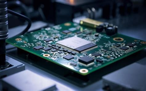
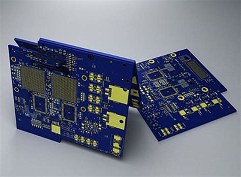
PCBs are complex assemblies of conductive tracks, pads, and other features etched from copper sheets laminated onto a non-conductive substrate. Faults can occur at any point in a PCB’s lifecycle – during manufacturing, assembly, or operation. Understanding these faults is crucial for effective repair.
Common causes of PCB failures include:
- Physical damage (impact, flexing)
- Thermal stress (overheating, thermal cycling)
- Electrical overload (short circuits, voltage spikes)
- Environmental factors (moisture, corrosion)
- Manufacturing defects (poor soldering, material flaws)
- Component failures (failed ICs, capacitors)
2. Common PCB Fault Types
2.1 Short Circuits
One of the most frequent and potentially damaging faults, short circuits occur when two or more points that should be at different potentials become connected. This can result from:
- Solder bridges between adjacent pads or tracks
- Conductive debris on the board surface
- Damaged insulation between layers in multilayer boards
- Component failures creating internal shorts
2.2 Open Circuits
The opposite of shorts, open circuits occur when continuity is broken in a circuit path. Causes include:
- Cracked or broken traces (often from mechanical stress)
- Failed vias (plated-through holes connecting layers)
- Poor solder joints (cold solder joints, cracked connections)
- Lifted pads (copper pads detached from the substrate)
2.3 Component Failures
Individual components can fail due to various reasons:
- Electrostatic discharge (ESD) damage
- Overvoltage or overcurrent conditions
- Thermal stress exceeding component ratings
- Aging (particularly electrolytic capacitors)
- Manufacturing defects
2.4 Intermittent Faults
These elusive faults appear and disappear, making diagnosis challenging:
- in traces or solder joints
- Loose connections
- Temperature-sensitive components
- Contamination that changes conductivity with humidity
3. Diagnostic Techniques
Effective PCB repair begins with accurate fault diagnosis. Here are key diagnostic methods:
3.1 Visual Inspection
The first and simplest step involves examining the PCB under good lighting, possibly with magnification:
- Look for burnt components or discolored areas
- Check for cracked or lifted components
- Inspect solder joints for cracks, voids, or insufficient solder
- Examine traces for damage or corrosion
- Look for bulging or leaking capacitors
3.2 Continuity Testing
Using a multimeter in continuity mode helps identify:
- Open circuits (no continuity where there should be)
- Short circuits (continuity where there shouldn’t be)
- Intermittent connections (by flexing the board during testing)
3.3 Power-On Testing
With proper precautions, powering the board can reveal:
- Overheating components (use thermal imaging or carefully feel)
- Voltage levels at test points (compare with schematic)
- Functional failures in specific circuit sections
3.4 Advanced Diagnostic Tools
For complex faults, specialized equipment may be needed:
- Oscilloscopes for signal analysis
- Logic analyzers for digital circuits
- X-ray inspection for hidden solder joints (BGA components)
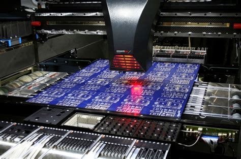
- Automated Optical Inspection (AOI) systems
- Flying probe testers for comprehensive connectivity checks
4. PCB Repair Techniques
Once faults are identified, appropriate repair methods can be applied:
4.1 Trace Repairs
Damaged copper traces can often be repaired:
- Clean the damaged area with isopropyl alcohol
- Remove damaged trace sections with a sharp blade
- Lightly abrade the area to remove solder mask
- Apply flux to the repair area
- Bridge the gap with solder or a small wire jumper
- For longer gaps, use specially made trace repair kits
- Protect the repair with conformal coating or epoxy
4.2 Pad and Via Repairs
Lifted or damaged pads and vias require careful attention:
- For through-hole components, use a via repair kit or insert a small wire through the hole and solder to adjacent traces
- Surface mount pads can sometimes be extended to adjacent copper areas
- Epoxy can help secure lifted pads before soldering
4.3 Solder Joint Repairs
Common solder joint issues and fixes:
- Cold solder joints: Reheat with fresh flux and additional solder
- Solder bridges: Use solder wick or a solder sucker to remove excess
- Cracked joints: Clean and resolder the connection
- Insufficient solder: Add fresh solder with proper heat
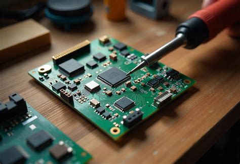
4.4 Component Replacement
When components fail:
- Desolder the faulty component using appropriate tools (solder wick, vacuum tools, or hot air)
- Clean the pad area thoroughly
- Position the new component correctly
- Apply fresh solder using proper technique
- For SMD components, use tweezers and possibly a microscope
4.5 Multilayer Board Repairs
Repairing inner layer faults is challenging but sometimes possible:
- For accessible inner layers, carefully drill to the fault and make repairs
- Sometimes external jumpers can bypass internal faults
- In complex cases, the board may need replacement
5. Specialized Repair Situations
5.1 BGA (Ball Grid Array) Rework
BGA components require special techniques:
- Use a preheater to gradually warm the entire board
- Apply precise hot air to the BGA area
- Use a vacuum tool or tweezers to remove the component
- Clean the pad area with solder wick
- Apply new solder balls or paste
- Precisely align and reflow the new component
5.2 Flexible PCB Repairs
Flex circuits present unique challenges:
- Use low-temperature soldering to avoid damaging the substrate
- Special conductive adhesives can sometimes replace solder
- Reinforcement may be needed at stress points
- Kapton tape can protect repaired areas
5.3 High-Frequency Circuit Repairs
RF and high-speed digital circuits need extra care:
- Maintain proper trace impedance during repairs
- Minimize the length of any repair jumpers
- Use shielding techniques where needed
- Be aware of signal integrity issues
6. Repair Equipment and Materials
A well-equipped PCB repair station includes:
- Temperature-controlled soldering iron with various tips
- Hot air rework station
- Quality multimeter
- Magnification (microscope or magnifying lamp)
- ESD-safe work area and tools
- Solder wick and solder suckers
- Precision tweezers and tools
- Flux in various forms (paste, liquid, pen)
- Quality solder (appropriate alloy and diameter)
- Conformal coating materials
- Epoxy and adhesives for mechanical repairs
7. Safety Considerations
PCB repair involves several hazards:
- Electrical safety when working on powered boards
- Toxic fumes from solder and flux (use fume extraction)
- Sharp tools and edges
- Hot surfaces and materials
- ESD protection for sensitive components
- Proper disposal of hazardous materials
Always:
- Work in a well-ventilated area
- Use personal protective equipment as needed
- Follow manufacturer safety guidelines
- Be aware of high-voltage areas in some boards
8. Preventive Measures and Best Practices
Many PCB failures can be prevented:
8.1 Design Considerations
- Adequate trace widths for current loads
- Proper spacing to prevent arcing
- Strain relief for connectors
- Thermal management in high-power areas
- Protection circuits (overvoltage, ESD)
8.2 Manufacturing Quality
- Proper solder paste application
- Adequate reflow profiles
- Thorough cleaning to remove flux residues
- Conformal coating where appropriate
8.3 Operational Considerations
- Proper cooling and ventilation
- Protection from moisture and contaminants
- Careful handling to prevent mechanical stress
- Regular maintenance and inspection
9. When Repair Isn’t Practical
Sometimes PCB repair isn’t cost-effective or technically feasible:
- Extensive damage to multilayer boards
- Advanced components that can’t be properly reworked
- When the repair cost approaches replacement cost
- Safety-critical applications where reliability is paramount
- Obsolete boards where replacements aren’t available
In these cases, complete board replacement or redesign may be necessary.
10. Future Trends in PCB Repair
Emerging technologies are changing PCB repair:
- 3D printing of circuit traces for repairs
- Advanced materials that self-heal minor damage
- AI-assisted fault diagnosis systems
- Improved portable repair tools
- Enhanced non-destructive testing methods
11. Conclusion
PCB fault repair is a critical skill in electronics maintenance and manufacturing. By understanding common failure modes, employing systematic diagnostic approaches, and applying appropriate repair techniques, many PCBs can be returned to service reliably and cost-effectively. As electronics continue to evolve, so too will repair methodologies, but the fundamental principles of careful observation, methodical troubleshooting, and precision workmanship will remain essential.
Whether you’re an electronics hobbyist, a field service technician, or a manufacturing engineer, developing strong PCB repair skills can save significant time and money while extending the life of valuable electronic equipment. With the right knowledge, tools, and patience, even complex PCB faults can often be successfully repaired.