PCB Filters: Design, Applications, and Advancements
Introduction
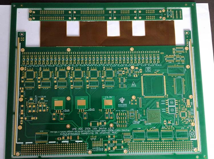
Printed Circuit Board (PCB) filters are essential components in modern electronic systems, playing a critical role in signal processing and noise reduction. As electronic devices become more compact and complex, the demand for efficient, reliable, and miniaturized filters has grown significantly. PCB filters, which are integrated directly onto the PCB, offer a cost-effective and space-saving solution for filtering unwanted signals and ensuring the integrity of desired signals. This article explores the design principles, applications, and recent advancements in PCB filter technology.
1. Fundamentals of PCB Filters
1.1 What is a PCB Filter?
A PCB filter is an electronic circuit integrated onto a printed circuit board that allows certain frequencies to pass while attenuating others. Filters are used to remove noise, interference, and unwanted signals from electronic systems, ensuring that only the desired signals are processed. PCB filters can be designed to operate in various frequency ranges, from low-frequency audio signals to high-frequency radio waves.
1.2 Types of PCB Filters
There are several types of PCB filters, each suited to specific applications:
- Low-Pass Filters (LPF): Allow signals with frequencies below a certain cutoff frequency to pass through while attenuating higher frequencies.
- High-Pass Filters (HPF): Allow signals with frequencies above a certain cutoff frequency to pass through while attenuating lower frequencies.
- Band-Pass Filters (BPF): Allow signals within a specific frequency range to pass through while attenuating frequencies outside this range.
- Band-Stop Filters (BSF): Attenuate signals within a specific frequency range while allowing frequencies outside this range to pass through.
- Notch Filters: A type of band-stop filter that targets a very narrow frequency range, often used to remove specific interference signals.
1.3 Filter Design Parameters
The design of a PCB filter involves several key parameters:
- Cutoff Frequency: The frequency at which the filter begins to attenuate the signal.
- Passband: The range of frequencies that the filter allows to pass through with minimal attenuation.
- Stopband: The range of frequencies that the filter attenuates.
- Insertion Loss: The loss of signal power resulting from the insertion of the filter in the signal path.
- Quality Factor (Q): A measure of the filter’s selectivity, indicating how sharply it can distinguish between the passband and stopband.
2. Design Considerations for PCB Filters
2.1 Material Selection
The choice of PCB material is crucial in filter design, as it affects the filter’s performance, especially at high frequencies. Key material properties to consider include:
- Dielectric Constant (εr): Determines the speed at which signals propagate through the material. A higher dielectric constant allows for smaller PCB dimensions but may increase signal loss.
- Loss Tangent (tan δ): Indicates the amount of signal loss due to the dielectric material. Lower loss tangents are preferred for high-frequency applications.
- Thermal Stability: Ensures that the filter’s performance remains consistent across varying temperatures.
Common PCB materials used in filter design include FR-4, Rogers, and Teflon, each offering different trade-offs between cost, performance, and manufacturability.
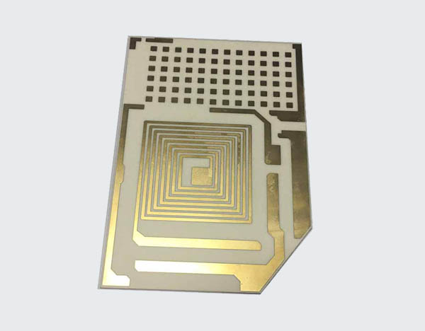
2.2 Topology and Layout
The physical layout of the filter on the PCB is critical to its performance. Key considerations include:
- Component Placement: Proper placement of components such as resistors, capacitors, and inductors is essential to minimize parasitic effects and ensure optimal filter performance.
- Trace Routing: Careful routing of signal traces helps to reduce crosstalk, electromagnetic interference (EMI), and signal reflections.
- Grounding: A solid ground plane is necessary to provide a stable reference point and minimize noise.
2.3 Simulation and Optimization
Before manufacturing, PCB filters are typically simulated using software tools to predict their performance and identify potential issues. Common simulation techniques include:
- S-Parameter Analysis: Used to evaluate the filter’s frequency response and insertion loss.
- Electromagnetic Simulation: Helps to model the effects of the PCB layout on the filter’s performance, including parasitic capacitance and inductance.
- Optimization Algorithms: Automated tools can be used to fine-tune the filter design, adjusting component values and layout to achieve the desired performance.
3. Applications of PCB Filters
3.1 Telecommunications
In telecommunications, PCB filters are used to separate different frequency bands, ensuring that signals are transmitted and received without interference. For example, in mobile phones, PCB filters are used to isolate the desired signal from the noise generated by other electronic components.
3.2 Audio Processing
In audio systems, PCB filters are used to shape the frequency response of audio signals. Low-pass filters are commonly used in subwoofers to remove high-frequency noise, while high-pass filters are used in tweeters to remove low-frequency signals.
3.3 Power Electronics
In power electronics, PCB filters are used to suppress electromagnetic interference (EMI) generated by switching devices such as transistors and diodes. These filters help to ensure compliance with regulatory standards and prevent interference with other electronic devices.
3.4 Medical Devices
In medical devices, PCB filters are used to process signals from sensors and other electronic components. For example, in an electrocardiogram (ECG) machine, PCB filters are used to remove noise from the electrical signals generated by the heart, ensuring accurate diagnosis.
3.5 Automotive Electronics
In automotive electronics, PCB filters are used to reduce noise and interference in various systems, including engine control units (ECUs), infotainment systems, and advanced driver-assistance systems (ADAS). These filters help to ensure reliable operation in the harsh electromagnetic environment of a vehicle.
4. Recent Advancements in PCB Filter Technology
4.1 Miniaturization
As electronic devices continue to shrink in size, there is a growing demand for miniaturized PCB filters. Advances in manufacturing techniques, such as multilayer PCBs and embedded components, have enabled the development of compact filters that can be integrated into increasingly small devices.
4.2 High-Frequency Filters
With the advent of 5G and other high-frequency communication technologies, there is a need for PCB filters that can operate at higher frequencies. Recent advancements in materials and design techniques have led to the development of filters capable of operating in the millimeter-wave range, enabling faster and more reliable communication.
4.3 Tunable Filters
Tunable PCB filters, which can adjust their frequency response dynamically, are becoming increasingly popular in applications where the operating frequency may vary. These filters use components such as varactors or microelectromechanical systems (MEMS) to adjust the filter’s characteristics in real-time, providing greater flexibility and performance.
4.4 Integration with Active Components
Traditionally, PCB filters have been passive components, relying on resistors, capacitors, and inductors to achieve the desired frequency response. However, recent advancements have led to the integration of active components, such as operational amplifiers, into PCB filters. This allows for greater control over the filter’s characteristics and can improve performance in certain applications.
4.5 Advanced Materials
The development of new materials with improved dielectric properties has enabled the creation of PCB filters with lower loss and higher performance. For example, the use of liquid crystal polymer (LCP) and other advanced materials has allowed for the design of filters that can operate at higher frequencies with minimal signal loss.
5. Challenges and Future Directions
5.1 Thermal Management
As PCB filters become more compact and operate at higher frequencies, thermal management becomes a critical challenge. The heat generated by the filter can affect its performance and reliability, necessitating the development of new cooling techniques and materials.
5.2 Signal Integrity
Maintaining signal integrity in high-frequency PCB filters is a significant challenge, as parasitic effects and signal reflections can degrade performance. Future advancements in design and simulation tools will be essential to address these issues.
5.3 Cost and Manufacturability
While advancements in PCB filter technology have enabled new capabilities, they have also increased the complexity and cost of manufacturing. Balancing performance with cost and manufacturability will be a key challenge for future developments.
5.4 Integration with Other Technologies
As electronic systems become more complex, there is a growing need for PCB filters that can be seamlessly integrated with other technologies, such as antennas, sensors, and power management systems. Future advancements will likely focus on creating more integrated and multifunctional PCB filters.
Conclusion
PCB filters are indispensable components in modern electronic systems, providing essential signal processing and noise reduction capabilities. As technology continues to evolve, the demand for more advanced, compact, and efficient PCB filters will only grow. By understanding the design principles, applications, and recent advancements in PCB filter technology, engineers can develop innovative solutions to meet the challenges of tomorrow’s electronic systems.