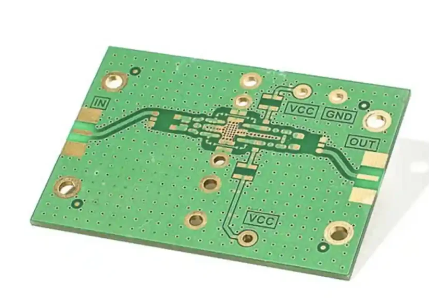
Pcb hdi fpc
Advantages Of Pcb hdi fpc In Modern Electronics
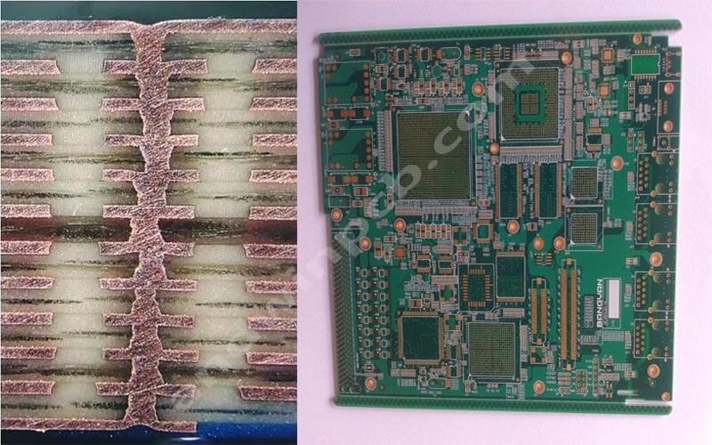
High-Density Interconnect (HDI) Printed Circuit Boards (PCBs) have become a cornerstone in the advancement of modern electronics, offering numerous advantages that cater to the ever-evolving demands of the industry. As electronic devices continue to shrink in size while increasing in functionality, the need for more efficient and compact circuit boards has never been more critical. HDI PCBs address this need by providing a higher wiring density per unit area compared to traditional PCBs, which translates into several key benefits.
One of the primary advantages of HDI PCBs is their ability to support miniaturization.
In an era where consumer electronics such as smartphones, tablets, and wearable devices are becoming increasingly compact, the reduced size of HDI PCBs allows for more components to be packed into a smaller space. This is achieved through the use of finer lines and spaces, smaller vias, and higher connection pad density. Consequently, manufacturers can design smaller, lighter, and more portable devices without compromising on performance or functionality.
In addition to supporting miniaturization, HDI PCBs enhance electrical performance.
The shorter distances between components reduce signal loss and improve signal integrity, which is crucial for high-speed applications. This is particularly important in telecommunications, computing, and automotive industries, where rapid data transmission and processing are essential. The improved electrical performance of HDI PCBs also contributes to lower power consumption, which is a significant advantage in battery-operated devices, extending their operational life.
Another notable benefit of HDI PCBs is their ability to facilitate complex designs.
The increased wiring density allows for more intricate and sophisticated circuit layouts, enabling the integration of advanced features and functionalities. This capability is especially valuable in the development of cutting-edge technologies such as 5G networks, Internet of Things (IoT) devices, and advanced medical equipment. By accommodating complex designs, HDI PCBs empower engineers to push the boundaries of innovation and create more powerful and versatile electronic products.
Moreover, HDI PCBs contribute to improved reliability and durability of electronic devices.
The use of microvias, which are smaller and more robust than traditional vias, enhances the mechanical strength of the board and reduces the risk of failure due to thermal and mechanical stress. This is particularly beneficial in applications that require high reliability, such as aerospace, military, and industrial electronics. The enhanced durability of HDI PCBs ensures that devices can withstand harsh operating conditions and maintain consistent performance over time.
Furthermore, HDI PCBs offer cost advantages in the long run.
Although the initial manufacturing cost of HDI PCBs may be higher due to the advanced fabrication techniques required, the overall cost-effectiveness is realized through the reduction in the number of layers needed for complex designs. This leads to savings in material costs and assembly time, ultimately resulting in a more economical solution for high-volume production.
In conclusion, the advantages of HDI PCBs in modern electronics are manifold, encompassing miniaturization, enhanced electrical performance, facilitation of complex designs, improved reliability, and long-term cost-effectiveness. As the demand for more compact, efficient, and sophisticated electronic devices continues to grow, HDI PCBs will undoubtedly play a pivotal role in shaping the future of the electronics industry. Their ability to meet the stringent requirements of contemporary applications makes them an indispensable component in the quest for technological advancement.
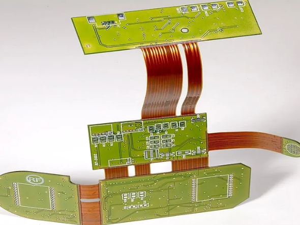
Design Considerations For Flexible Printed Circuits (FPC)
When designing Flexible Printed Circuits (FPC), several critical considerations must be taken into account to ensure optimal performance and reliability. FPCs, known for their flexibility, lightweight nature, and ability to fit into compact spaces, are increasingly utilized in various applications, from consumer electronics to medical devices. To achieve a successful design, engineers must carefully evaluate material selection, mechanical properties, electrical performance, and manufacturing processes.
Firstly, material selection is paramount in FPC design.
The choice of substrate material, typically polyimide or polyester, significantly impacts the circuit’s flexibility, thermal stability, and overall durability. Polyimide is often preferred due to its excellent thermal resistance and mechanical properties, making it suitable for high-temperature applications. Conversely, polyester is more cost-effective and adequate for lower-temperature environments. Additionally, the selection of conductive materials, such as copper, must be considered for their electrical conductivity and compatibility with the chosen substrate.
Transitioning to mechanical properties, the flexibility and bend radius of the FPC are crucial factors.
The bend radius, defined as the minimum radius the circuit can be bent without causing damage, must be carefully calculated to prevent mechanical failure. Engineers must consider the number of layers, thickness of the substrate, and the type of adhesive used in the construction of the FPC. A smaller bend radius can be achieved by using thinner substrates and strategically placing stiffeners to reinforce areas prone to stress. Moreover, dynamic flexing applications, where the circuit is repeatedly bent, require materials and designs that can withstand continuous mechanical stress without degradation.
In terms of electrical performance, signal integrity and impedance control are essential considerations.
High-speed applications necessitate precise impedance matching to minimize signal loss and electromagnetic interference (EMI). This can be achieved by carefully designing the trace width, spacing, and layer stack-up. Additionally, the use of ground planes and shielding techniques can further enhance signal integrity. Engineers must also account for the potential impact of environmental factors, such as temperature and humidity, on the electrical properties of the FPC.
Furthermore, the manufacturing process plays a significant role in the design of FPCs.
The choice of fabrication techniques, such as additive or subtractive processes, influences the resolution and accuracy of the circuit features. Additive processes, like screen printing or inkjet printing, allow for the deposition of conductive materials directly onto the substrate, offering greater design flexibility. Subtractive processes, such as etching, involve the removal of unwanted material to create the desired circuit pattern. Each method has its advantages and limitations, and the selection depends on the specific requirements of the application.
Additionally, the assembly process must be considered during the design phase.
Surface mount technology (SMT) and through-hole technology (THT) are commonly used for component attachment. The choice between these methods depends on factors such as component size, placement accuracy, and mechanical strength. Engineers must also ensure that the FPC design accommodates the thermal profiles required for soldering processes, as excessive heat can damage the flexible substrate.
In conclusion, designing Flexible Printed Circuits requires a comprehensive understanding of material properties, mechanical constraints, electrical performance, and manufacturing techniques. By carefully considering these factors, engineers can create reliable and efficient FPCs that meet the demands of various applications. The integration of advanced materials and innovative design approaches continues to push the boundaries of what is possible with flexible electronics, paving the way for new and exciting technological advancements.
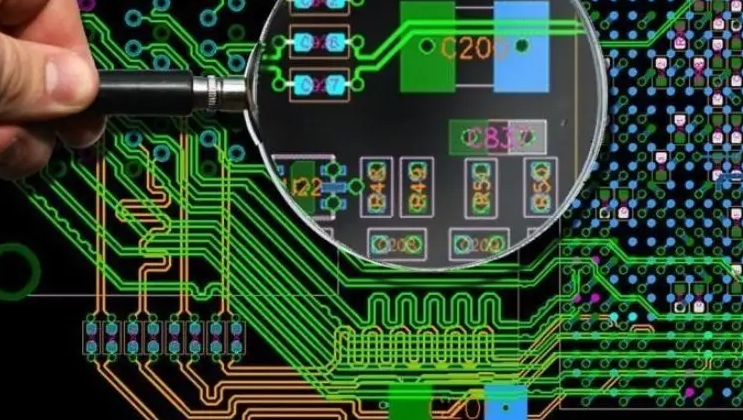
Comparing HDI And Traditional PCB Technologies
High-Density Interconnect (HDI) and traditional Printed Circuit Board (PCB) technologies represent two distinct approaches to electronic circuit design and manufacturing. As the demand for more compact, efficient, and high-performance electronic devices continues to grow, understanding the differences between these two technologies becomes increasingly important for engineers and designers.
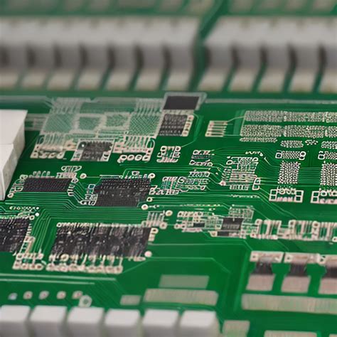
Traditional PCBs have been the backbone of electronic devices for decades.
They are typically constructed using a series of layers, including a substrate, conductive pathways, and insulating materials. These layers are laminated together to form a rigid board that can support various electronic components. Traditional PCBs are known for their reliability, ease of manufacturing, and cost-effectiveness, making them suitable for a wide range of applications, from consumer electronics to industrial machinery.
However, as electronic devices have become more sophisticated and miniaturized, the limitations of traditional PCBs have become more apparent.
One of the primary challenges is the inability to accommodate the increasing density of components and interconnections required by modern devices. This is where HDI technology comes into play.
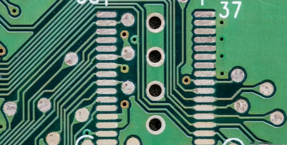
HDI PCBs are designed to address the limitations of traditional PCBs by incorporating advanced manufacturing techniques that allow for higher component density and more complex interconnections. One of the key features of HDI technology is the use of microvias, which are significantly smaller than the vias used in traditional PCBs. Microvias enable designers to create more intricate routing patterns, thereby increasing the overall density of the board. Additionally, HDI PCBs often utilize multiple layers of interconnections, known as stacked or staggered vias, which further enhance their ability to support complex designs.
Another significant advantage of HDI technology is its ability to reduce signal loss and improve overall performance.
The shorter interconnection paths and reduced parasitic inductance and capacitance in HDI PCBs result in better signal integrity and faster signal transmission. This makes HDI technology particularly well-suited for high-speed and high-frequency applications, such as telecommunications, aerospace, and advanced computing.
Despite these advantages, HDI technology also presents certain challenges.
The manufacturing process for HDI PCBs is more complex and requires specialized equipment and materials. This can result in higher production costs compared to traditional PCBs. Additionally, the design process for HDI PCBs is more intricate, requiring advanced software tools and a higher level of expertise. Consequently, the adoption of HDI technology may not be feasible for all applications, particularly those with budget constraints or less demanding performance requirements.
In contrast, traditional PCBs remain a viable option for many applications due to their simplicity, cost-effectiveness, and proven reliability.
For products that do not require the high density and performance capabilities of HDI technology, traditional PCBs offer a practical and efficient solution. Moreover, the well-established manufacturing processes and widespread availability of materials for traditional PCBs make them an attractive choice for many industries.
In conclusion, the choice between HDI and traditional PCB technologies depends on the specific requirements of the application. While HDI technology offers significant advantages in terms of component density, signal integrity, and overall performance, it also comes with higher costs and complexity. Traditional PCBs, on the other hand, provide a reliable and cost-effective solution for less demanding applications. By carefully considering the unique needs of their projects, designers and engineers can make informed decisions about which technology is best suited to their requirements.
Applications Of Flexible Printed Circuits In Wearable Devices
Flexible Printed Circuits (FPCs) have revolutionized the design and functionality of wearable devices, offering a myriad of applications that enhance both performance and user experience. As the demand for more compact, lightweight, and versatile electronic devices continues to grow, FPCs have emerged as a critical component in the development of next-generation wearables. These circuits, characterized by their flexibility, thinness, and durability, provide significant advantages over traditional rigid printed circuit boards (PCBs), particularly in the context of wearable technology.
One of the primary applications of FPCs in wearable devices is in the realm of fitness trackers and smartwatches.
These devices require a high degree of flexibility to conform to the contours of the human body while maintaining robust electrical performance. FPCs enable the integration of various sensors, such as heart rate monitors, accelerometers, and gyroscopes, into a single, flexible substrate. This integration not only reduces the overall weight and size of the device but also enhances its durability and reliability. Moreover, the flexibility of these circuits allows for more innovative and ergonomic designs, improving user comfort and wearability.
In addition to fitness trackers and smartwatches, FPCs are also extensively used in medical wearables.
These devices, which include continuous glucose monitors, ECG monitors, and wearable drug delivery systems, benefit greatly from the properties of flexible circuits. The ability of FPCs to bend and stretch without compromising electrical integrity is crucial for medical applications, where devices must adhere closely to the skin and withstand the rigors of daily use. Furthermore, the miniaturization enabled by FPCs allows for the development of less intrusive and more discreet medical wearables, thereby improving patient compliance and overall quality of life.
Transitioning from medical to consumer electronics, FPCs play a vital role in the development of smart clothing and e-textiles.
These innovative garments incorporate electronic components directly into the fabric, enabling functionalities such as biometric monitoring, temperature regulation, and even interactive lighting. The flexibility and thin profile of FPCs make them ideal for integration into textiles, where they can be woven or laminated without adding significant bulk or weight. This seamless integration of electronics into clothing opens up new possibilities for fashion, sports, and healthcare industries, providing users with enhanced functionality and convenience.
Moreover, the use of FPCs extends to the realm of augmented reality (AR) and virtual reality (VR) wearables.
Devices such as AR glasses and VR headsets require intricate circuitry to support high-resolution displays, sensors, and connectivity modules. FPCs offer the necessary flexibility and compactness to accommodate these components within the limited space available in such devices. This not only improves the overall design and aesthetics but also enhances the user experience by providing a more comfortable and immersive interface.
In conclusion, the applications of Flexible Printed Circuits in wearable devices are vast and varied, spanning fitness trackers, medical wearables, smart clothing, and AR/VR devices. The unique properties of FPCs, including their flexibility, thinness, and durability, make them indispensable in the development of modern wearables. As technology continues to advance, the role of FPCs in wearable devices is expected to grow, driving further innovation and improving the functionality and user experience of these cutting-edge products.