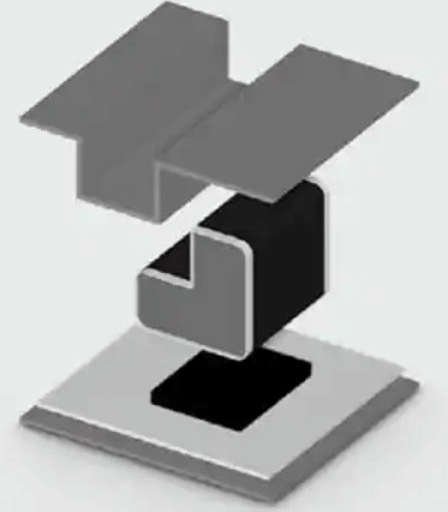
Pcb hdi pth
Advantages Of HDI PCBs In Modern Electronics
High-Density Interconnect (HDI) Printed Circuit Boards (PCBs) have become a cornerstone in the advancement of modern electronics, offering a multitude of advantages that cater to the ever-evolving demands of the industry. As electronic devices continue to shrink in size while increasing in functionality, the need for more sophisticated and efficient PCB designs has never been more critical. HDI PCBs, characterized by their higher wiring density per unit area compared to traditional PCBs, address these needs through several key benefits.
One of the primary advantages of HDI PCBs is their ability to support miniaturization.
In an era where compactness is paramount, HDI technology allows for the integration of more components in a smaller footprint. This is achieved through the use of finer lines and spaces, smaller vias, and higher connection pad density. Consequently, devices such as smartphones, tablets, and wearable technology can be designed to be more compact and lightweight without compromising on performance or functionality. This miniaturization also extends to medical devices, where smaller, more efficient electronics can lead to less invasive procedures and more portable diagnostic tools.
In addition to enabling smaller device sizes, HDI PCBs enhance electrical performance.
The reduced distance between components and the use of microvias, which are smaller than traditional vias, result in lower signal loss and faster signal transmission. This is particularly beneficial in high-speed applications where signal integrity is crucial. For instance, in telecommunications and data processing, the ability to maintain high signal quality over shorter distances can lead to more reliable and faster communication systems. Furthermore, the improved electrical performance of HDI PCBs supports the development of advanced computing systems, where rapid data processing and minimal latency are essential.
Another significant advantage of HDI PCBs is their contribution to increased reliability and durability.
The use of multiple layers and microvias not only allows for more complex routing but also enhances the mechanical strength of the board. This is particularly important in applications where the PCB is subjected to harsh conditions, such as in automotive and aerospace industries. The robust construction of HDI PCBs ensures that they can withstand extreme temperatures, vibrations, and other environmental stresses, thereby extending the lifespan of the electronic device.
Moreover, HDI PCBs facilitate better thermal management.
The dense component placement and multiple layers enable efficient heat dissipation, which is critical in preventing overheating and ensuring the stable operation of electronic devices. Effective thermal management is essential in high-power applications, such as power supplies and LED lighting, where excessive heat can lead to performance degradation and potential failure. By incorporating HDI technology, manufacturers can design PCBs that maintain optimal operating temperatures, thereby enhancing the overall reliability and efficiency of the device.
In conclusion, the advantages of HDI PCBs in modern electronics are manifold, ranging from enabling miniaturization and enhancing electrical performance to increasing reliability and improving thermal management. As the demand for more compact, efficient, and high-performing electronic devices continues to grow, the role of HDI PCBs will undoubtedly become even more pivotal. By leveraging the benefits of HDI technology, manufacturers can meet the stringent requirements of contemporary electronic applications, paving the way for continued innovation and advancement in the industry.
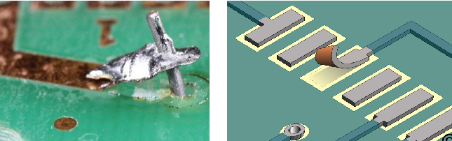
Key Differences Between HDI And PTH PCBs
Printed Circuit Boards (PCBs) are the backbone of modern electronic devices, and their design and manufacturing processes have evolved significantly over the years. Among the various types of PCBs, High-Density Interconnect (HDI) and Plated Through-Hole (PTH) PCBs are two prominent categories that serve different purposes and applications. Understanding the key differences between HDI and PTH PCBs is crucial for selecting the appropriate type for specific electronic projects.
To begin with, HDI PCBs are characterized by their high wiring density per unit area, which is achieved through the use of microvias, blind vias, and buried vias.
These advanced interconnect techniques allow for more complex and compact designs, making HDI PCBs ideal for applications where space is at a premium, such as in smartphones, tablets, and other portable electronic devices. In contrast, PTH PCBs utilize through-hole technology, where holes are drilled through the entire thickness of the board and plated to create electrical connections between different layers. This traditional method is well-suited for applications that require robust mechanical connections, such as in industrial equipment and large-scale electronic systems.
One of the primary differences between HDI and PTH PCBs lies in their manufacturing processes.
HDI PCBs require advanced fabrication techniques, including laser drilling for microvias and sequential lamination for creating multiple layers. These processes enable the production of finer lines and spaces, allowing for higher component density and improved electrical performance. On the other hand, PTH PCBs are manufactured using conventional drilling and plating methods, which are less complex and more cost-effective. However, the larger vias and wider traces in PTH PCBs limit their ability to support high-density designs.
Another significant distinction is the aspect of signal integrity.
HDI PCBs offer superior signal integrity due to their shorter interconnect paths and reduced parasitic inductance and capacitance. This makes them suitable for high-speed and high-frequency applications, where maintaining signal quality is critical. Conversely, PTH PCBs, with their longer interconnect paths and larger vias, may experience greater signal degradation, making them less ideal for such demanding applications.
Thermal management is also a crucial factor to consider when comparing HDI and PTH PCBs.
HDI PCBs, with their thinner dielectric layers and higher copper density, provide better heat dissipation, which is essential for preventing overheating in densely packed electronic assemblies. PTH PCBs, while generally having thicker dielectric layers, may not offer the same level of thermal performance, potentially leading to heat-related issues in high-power applications.
Furthermore, the choice between HDI and PTH PCBs can impact the overall cost and time-to-market of a project.
HDI PCBs, with their advanced manufacturing requirements, tend to be more expensive and have longer lead times compared to PTH PCBs. This cost factor must be weighed against the benefits of higher performance and miniaturization that HDI technology offers. In contrast, PTH PCBs, being simpler and more established, provide a cost-effective solution for less demanding applications, with shorter production cycles.
In conclusion, the key differences between HDI and PTH PCBs revolve around their design complexity, manufacturing processes, signal integrity, thermal management, and cost considerations. HDI PCBs are well-suited for high-density, high-performance applications where space and signal quality are paramount, while PTH PCBs offer a robust and cost-effective solution for applications requiring strong mechanical connections and less stringent performance requirements. Understanding these distinctions is essential for making informed decisions in the design and selection of PCBs for various electronic projects.
Design Considerations For HDI PCBs
High-Density Interconnect (HDI) Printed Circuit Boards (PCBs) have become a cornerstone in modern electronics, offering enhanced performance and miniaturization capabilities. As the demand for more compact and efficient electronic devices grows, the design considerations for HDI PCBs become increasingly critical. One of the primary aspects to consider is the layer stack-up, which involves determining the number of layers and their arrangement. This decision impacts the board’s overall performance, signal integrity, and manufacturability. A well-planned layer stack-up can minimize electromagnetic interference (EMI) and ensure robust power distribution.
Transitioning to the aspect of via technology, HDI PCBs often employ microvias, blind vias, and buried vias to achieve higher component density.
Microvias, in particular, are essential for connecting different layers without consuming much space. However, the choice of via type must be carefully evaluated based on the specific application requirements and manufacturing capabilities. For instance, microvias are typically limited to a depth of one layer, necessitating a strategic approach to layer interconnections.
Another crucial consideration is the selection of materials.
The dielectric materials used in HDI PCBs must exhibit low dielectric constant and low loss tangent to support high-frequency signal transmission. Additionally, the thermal properties of the materials are vital, especially in applications involving high power or high-speed signals. Materials with high thermal conductivity can effectively dissipate heat, thereby enhancing the reliability and longevity of the PCB.
Signal integrity is another paramount factor in HDI PCB design.
As signal speeds increase, issues such as crosstalk, signal attenuation, and reflection become more pronounced. To mitigate these issues, designers must carefully route high-speed signals, maintain consistent impedance, and use proper termination techniques. Differential pair routing and controlled impedance traces are commonly employed strategies to preserve signal integrity.
Power integrity is equally important, particularly in densely packed HDI PCBs.
Ensuring a stable power supply to all components requires meticulous planning of power and ground planes. The use of multiple power and ground layers can help reduce noise and provide a low-impedance path for return currents. Decoupling capacitors should be strategically placed to filter out noise and stabilize the power supply.
Thermal management is another critical aspect that cannot be overlooked.
As electronic devices become more compact, the heat generated by components can lead to performance degradation or even failure. Effective thermal management strategies, such as the use of thermal vias, heat sinks, and thermal interface materials, are essential to dissipate heat and maintain optimal operating temperatures.
Manufacturability is a practical consideration that influences the overall design process.
While HDI PCBs offer numerous advantages, they also present manufacturing challenges. The precision required for drilling microvias, the alignment of multiple layers, and the handling of fine-pitch components necessitate advanced manufacturing techniques and equipment. Collaborating closely with PCB manufacturers during the design phase can help identify potential issues and ensure a smooth production process.
In conclusion, designing HDI PCBs involves a complex interplay of various factors, including layer stack-up, via technology, material selection, signal and power integrity, thermal management, and manufacturability. Each of these considerations must be meticulously addressed to achieve a high-performance, reliable, and manufacturable PCB. As technology continues to evolve, staying abreast of the latest advancements and best practices in HDI PCB design will be essential for engineers and designers striving to meet the ever-increasing demands of modern electronic devices.
Applications Of PTH PCBs In Industrial Electronics
In the realm of industrial electronics, the application of Plated Through-Hole (PTH) Printed Circuit Boards (PCBs) has become increasingly significant. These PCBs, characterized by their through-hole technology, offer a robust and reliable solution for various industrial applications. The versatility and durability of PTH PCBs make them indispensable in environments where mechanical stress and high reliability are paramount.
One of the primary applications of PTH PCBs in industrial electronics is in the manufacturing of heavy machinery.
These machines often operate under extreme conditions, including high temperatures, vibrations, and mechanical shocks. PTH PCBs are well-suited for such environments due to their strong mechanical bonds, which are achieved through the plating process. This ensures that the components remain securely attached to the board, thereby enhancing the overall reliability and longevity of the machinery.
Moreover, PTH PCBs are extensively used in the production of industrial control systems.
These systems are critical for the automation and control of various industrial processes. The reliability of PTH PCBs ensures that these control systems can operate continuously without failure, which is crucial for maintaining the efficiency and safety of industrial operations. The ability of PTH PCBs to handle high current loads and their excellent thermal management properties further contribute to their suitability for such applications.
In addition to heavy machinery and control systems, PTH PCBs find applications in power supply units.
Industrial power supplies require PCBs that can handle high power levels and provide stable and reliable performance. PTH PCBs, with their superior electrical conductivity and ability to support large components, are ideal for these requirements. They ensure that the power supply units can deliver consistent power to various industrial equipment, thereby preventing downtime and enhancing productivity.
Furthermore, the use of PTH PCBs extends to the field of industrial communication systems.
These systems are essential for the seamless exchange of information between different parts of an industrial setup. PTH PCBs provide the necessary reliability and durability to ensure that communication systems function without interruption. Their ability to support complex circuitry and multiple layers makes them suitable for advanced communication devices that require high-speed data transmission and robust performance.
Another notable application of PTH PCBs is in the development of industrial sensors and instrumentation.
These devices are crucial for monitoring and controlling various parameters within an industrial environment. PTH PCBs offer the precision and reliability needed for accurate sensor readings and consistent performance of instrumentation devices. Their ability to withstand harsh conditions and provide stable electrical connections ensures that industrial sensors and instruments can operate effectively over extended periods.
In conclusion, the applications of PTH PCBs in industrial electronics are vast and varied. Their robust construction, reliability, and ability to handle high power and complex circuitry make them an essential component in heavy machinery, control systems, power supply units, communication systems, and industrial sensors. As industrial processes continue to evolve and demand higher levels of efficiency and reliability, the role of PTH PCBs in supporting these advancements will undoubtedly remain crucial. The continued development and innovation in PTH PCB technology will further enhance their applications, ensuring that they remain at the forefront of industrial electronics.