PCB Industry Solutions: Driving Innovation in Electronics Manufacturing
Introduction
The Printed Circuit Board (PCB) industry is the backbone of modern electronics, enabling the functionality of devices ranging from smartphones to aerospace systems. As technology advances, the demand for more complex, efficient, and reliable PCBs grows. To meet these challenges, the PCB industry has developed innovative solutions in design, manufacturing, materials, and testing. This article explores key PCB industry solutions that enhance performance, reduce costs, and support sustainability.
1. Advanced PCB Design Solutions
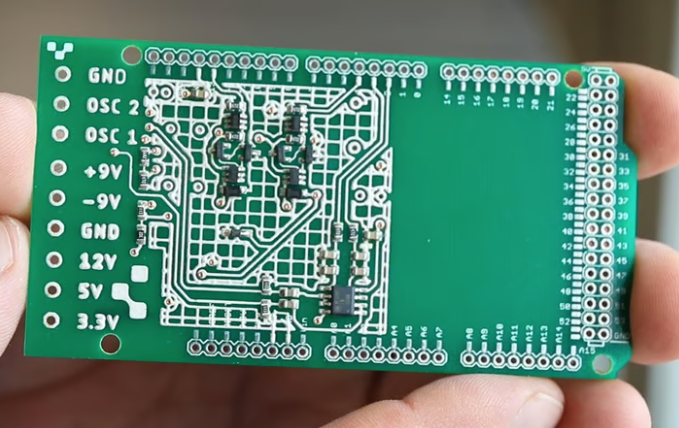
1.1 High-Density Interconnect (HDI) Technology
HDI PCBs allow for finer lines, smaller vias, and higher connection density, making them ideal for compact devices like smartphones and wearables. Benefits include:
- Improved signal integrity
- Reduced size and weight
- Enhanced thermal management
1.2 Flexible and Rigid-Flex PCBs
Flexible PCBs (FPCBs) and rigid-flex PCBs enable bendable and foldable electronics, widely used in medical devices, automotive systems, and IoT applications. Key advantages:
- Space-saving designs
- Increased durability in dynamic environments
- Better resistance to vibrations and shocks
1.3 AI and Machine Learning in PCB Design
AI-powered design tools optimize PCB layouts by:
- Automating routing and component placement
- Predicting signal interference and thermal issues
- Reducing design iteration time
2. Innovative Manufacturing Techniques
2.1 Additive Manufacturing (3D Printing)
3D-printed PCBs are gaining traction due to:
- Rapid prototyping capabilities
- Customizable designs without traditional etching
- Reduced material waste
2.2 Automated Optical Inspection (AOI) and AI-Based Defect Detection
Automated inspection systems improve quality control by:
- Detecting micro-defects (e.g., soldering errors, misalignments)
- Reducing human error in visual inspections
- Enhancing yield rates in mass production
2.3 Laser Direct Imaging (LDI)
LDI replaces traditional photolithography with laser-based patterning, offering:
- Higher precision for fine-line PCBs
- Faster production cycles
- Lower chemical usage, supporting eco-friendly manufacturing
3. Advanced Materials for Enhanced Performance
3.1 High-Frequency and Low-Loss Materials
For 5G, IoT, and RF applications, specialized materials like PTFE and ceramic-filled laminates provide:
- Lower signal loss at high frequencies
- Improved thermal stability
- Better impedance control
3.2 Thermal Management Solutions
Advanced thermal substrates (e.g., metal-core PCBs, insulated metal substrates) help dissipate heat in high-power applications such as LEDs and automotive electronics.
3.3 Sustainable and Eco-Friendly Materials
With increasing environmental regulations, the industry is adopting:
- Halogen-free laminates
- Lead-free soldering techniques
- Recyclable PCB materials
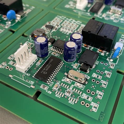
4. Smart Testing and Quality Assurance
4.1 In-Circuit Testing (ICT) and Flying Probe Testing
- ICT checks electrical performance at the component level.
- Flying probe testing is ideal for small-batch and high-mix production.
4.2 Automated X-Ray Inspection (AXI)
AXI detects hidden defects in multilayer PCBs, such as:
- Voiding in solder joints
- Barrel cracks in vias
- Misaligned internal layers
4.3 IoT-Enabled Predictive Maintenance
Smart factories use IoT sensors to monitor PCB manufacturing equipment, predicting failures and minimizing downtime.
5. Industry 4.0 and Smart Manufacturing
5.1 Digital Twin Technology
Digital twins simulate PCB production processes, enabling:
- Virtual testing before physical manufacturing
- Optimization of production workflows
- Faster time-to-market
5.2 Robotics and Automation in PCB Assembly
Robotic arms and pick-and-place machines enhance precision and speed in PCB assembly, reducing labor costs.
5.3 Blockchain for Supply Chain Transparency
Blockchain ensures traceability of PCB materials, preventing counterfeit components and improving compliance.
6. Challenges and Future Trends
6.1 Miniaturization and Complexity
As PCBs shrink, challenges include:
- Managing signal integrity in ultra-HDI designs
- Ensuring reliability in high-temperature environments
6.2 Sustainability and Circular Economy
The industry is shifting toward:
- Green manufacturing processes
- Recycling end-of-life PCBs
- Reducing hazardous substances
6.3 Emerging Technologies
Future PCB innovations may involve:
- Embedded components (resistors, capacitors inside the PCB)
- Quantum computing-compatible PCBs
- Biodegradable substrates for disposable electronics
Conclusion
The PCB industry continues to evolve with cutting-edge solutions in design, materials, manufacturing, and testing. By embracing AI, automation, and sustainable practices, PCB manufacturers can meet the growing demands of next-generation electronics. As technology progresses, the industry must balance innovation with environmental responsibility to ensure long-term growth.
With these advancements, PCBs will remain a critical enabler of the digital revolution, powering everything from consumer gadgets to industrial automation and beyond.