PCB Layout: A Comprehensive Guide to Optimizing Performance and Manufacturability
Printed Circuit Board (PCB) layout is a critical phase in the design of electronic systems, where the physical arrangement of components and routing of electrical connections are determined. A well-designed PCB layout ensures optimal electrical performance, thermal management, and manufacturability, while a poor layout can lead to signal integrity issues, electromagnetic interference (EMI), and production challenges. This article provides a comprehensive guide to PCB layout, covering key principles, design considerations, best practices, and advanced techniques to help engineers create high-performance and reliable PCBs.
1. Introduction to PCB Layout
PCB layout is the process of arranging components and routing traces on a PCB to create a functional electronic circuit. It involves translating the schematic design into a physical layout that meets electrical, thermal, and mechanical requirements. The layout process requires careful consideration of factors such as signal integrity, power distribution, thermal management, and manufacturability. A well-executed PCB layout ensures that the final product performs reliably under its intended operating conditions.
2. Key Principles of PCB Layout
2.1 Signal Integrity
Signal integrity refers to the quality of electrical signals as they travel through the PCB. Poor signal integrity can lead to issues such as signal reflections, crosstalk, and timing errors. Key considerations include:
- Impedance Matching: Ensure that the impedance of transmission lines matches the source and load impedances to minimize reflections.
- Trace Length: Minimize trace lengths for high-speed signals to reduce signal degradation.
- Routing Topology: Use appropriate routing topologies (e.g., daisy chain, star) to ensure consistent signal timing.
2.2 Power Integrity
Power integrity ensures that all components receive stable and sufficient power. Poor power distribution can lead to voltage drops, noise, and circuit malfunctions. Key considerations include:
- Power Planes: Use dedicated power and ground planes to provide low-impedance power distribution.
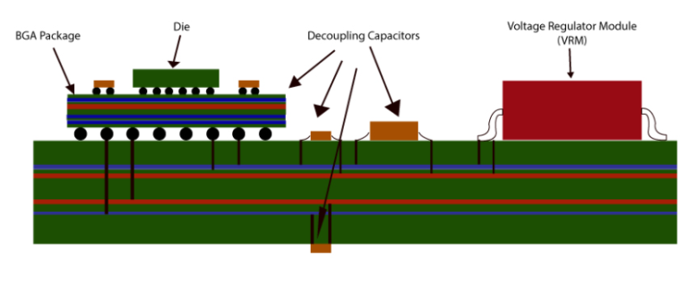
- Decoupling Capacitors: Place decoupling capacitors close to power pins to filter noise and stabilize voltage.
- Trace Width: Use wide traces for power lines to minimize resistance and voltage drop.
2.3 Thermal Management
Thermal management is critical for preventing overheating and ensuring the reliability of components. Key considerations include:
- Component Placement: Place heat-generating components away from sensitive components and near thermal vias or heat sinks.
- Thermal Vias: Use thermal vias to transfer heat from components to the inner layers or the opposite side of the PCB.
- Copper Pour: Increase the copper area around heat-generating components to improve heat dissipation.
2.4 Electromagnetic Compatibility (EMC)
EMC ensures that the PCB does not emit excessive electromagnetic interference (EMI) and is immune to external interference. Key considerations include:
- Grounding: Use a solid ground plane to reduce ground loops and noise.
- Shielding: Use shielding techniques, such as grounded copper pours or metal enclosures, to block EMI.
- Trace Routing: Avoid routing high-speed signals near sensitive components or parallel to other traces to minimize crosstalk.

3. PCB Layout Design Considerations
3.1 Component Placement
Component placement is the first step in PCB layout and has a significant impact on the overall design. Key guidelines include:
- Functional Grouping: Group related components together to minimize trace lengths and improve signal integrity.
- Orientation: Orient components to simplify routing and minimize crossing traces.
- Mechanical Constraints: Consider mechanical constraints, such as enclosure size and mounting holes, when placing components.
3.2 Routing
Routing involves connecting components with copper traces. Key considerations include:
- Trace Width: Use appropriate trace widths based on current requirements and impedance control.
- Trace Spacing: Maintain sufficient spacing between traces to prevent crosstalk and short circuits.
- Layer Stackup: Use multiple layers to separate signal, power, and ground planes, reducing noise and improving signal integrity.
3.3 Via Design
Vias are used to connect traces on different layers. Key considerations include:
- Via Size: Use smaller vias for high-density designs but ensure they are manufacturable.
- Via Placement: Place vias close to components to minimize trace lengths and improve signal integrity.
- Thermal Vias: Use thermal vias to transfer heat from components to the inner layers or the opposite side of the PCB.
3.4 Power Distribution
Proper power distribution is essential for ensuring stable and sufficient power to all components. Key considerations include:
- Power Planes: Use dedicated power and ground planes to provide low-impedance power distribution.
- Decoupling Capacitors: Place decoupling capacitors close to power pins to filter noise and stabilize voltage.
- Trace Width: Use wide traces for power lines to minimize resistance and voltage drop.
4. Best Practices for PCB Layout
4.1 Follow Design Rules
Adhere to the PCB manufacturer’s design rules for trace width, spacing, via size, and other parameters to ensure manufacturability.
4.2 Use Design for Manufacturability (DFM) Principles
Design the PCB with manufacturability in mind, considering factors such as component placement, routing, and solder mask design.
4.3 Optimize Signal Integrity
- Impedance Matching: Ensure that the impedance of transmission lines matches the source and load impedances.
- Trace Length: Minimize trace lengths for high-speed signals to reduce signal degradation.
- Routing Topology: Use appropriate routing topologies to ensure consistent signal timing.
4.4 Ensure Proper Grounding
- Ground Plane: Use a solid ground plane to reduce ground loops and noise.
- Ground Vias: Place ground vias near components to minimize ground inductance.
- Split Ground Planes: Avoid splitting ground planes, as this can create ground loops and increase EMI.
4.5 Implement Thermal Management
- Component Placement: Place heat-generating components away from sensitive components and near thermal vias or heat sinks.
- Thermal Vias: Use thermal vias to transfer heat from components to the inner layers or the opposite side of the PCB.
- Copper Pour: Increase the copper area around heat-generating components to improve heat dissipation.
5. Advanced Techniques for PCB Layout
5.1 High-Density Interconnect (HDI)
HDI technology allows for higher component density and improved signal integrity, making it ideal for compact and high-performance designs. Techniques include microvias, blind/buried vias, and fine-pitch components.
5.2 Differential Pair Routing
Differential pair routing is used for high-speed signals to reduce noise and improve signal integrity. Key considerations include:
- Trace Length Matching: Ensure that the lengths of the differential pairs are matched to avoid skew.
- Trace Spacing: Maintain consistent spacing between the differential pairs to ensure proper impedance.
5.3 3D PCB Design
3D PCB design tools allow engineers to visualize and optimize the physical layout of components and traces, considering factors such as component height, enclosure size, and mechanical constraints.
6. Common Challenges and Solutions
6.1 Signal Integrity Issues
- Challenge: Signal reflections, crosstalk, and timing errors can degrade signal integrity.
- Solution: Use impedance matching, minimize trace lengths, and use appropriate routing topologies.
6.2 Power Distribution Problems
- Challenge: Voltage drops, noise, and insufficient power can lead to circuit malfunctions.
- Solution: Use dedicated power and ground planes, place decoupling capacitors close to power pins, and use wide traces for power lines.
6.3 Thermal Management Issues
- Challenge: Overheating can lead to component failure and reduced reliability.
- Solution: Place heat-generating components near thermal vias or heat sinks, use thermal vias, and increase the copper area around heat-generating components.
7. Emerging Trends in PCB Layout
7.1 Artificial Intelligence (AI) and Machine Learning
AI and machine learning are being used to optimize PCB layout, reducing design time and improving performance.
7.2 Flexible and Rigid-Flex PCBs
Flexible and rigid-flex PCBs are becoming more common, offering new possibilities for compact and innovative designs.
7.3 Advanced Materials
New materials, such as high-temperature laminates and low-loss dielectrics, are being developed to improve PCB performance and reliability.
8. Conclusion
PCB layout is a critical aspect of electronic design that requires careful consideration of signal integrity, power distribution, thermal management, and manufacturability. By following best practices and leveraging advanced techniques, engineers can create high-performance and reliable PCBs that meet the demands of modern electronics. Emerging trends, such as AI, flexible PCBs, and advanced materials, are shaping the future of PCB layout, offering new opportunities for innovation and performance enhancement. With careful attention to detail and adherence to industry standards, PCB layout can be optimized to deliver the reliability and performance needed to power the next generation of electronic devices.