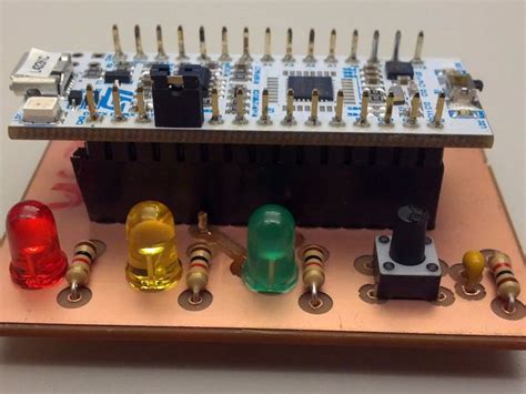
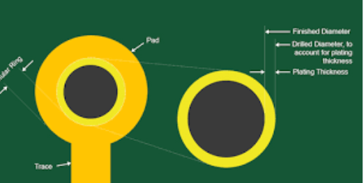
Pcb layout advice
Today’s switching regulators and power supplies are becoming more sophisticated and powerful, but one of the challenges is that the ever-increasing switching frequencies make design more difficult. Layout is becoming the difference between a good switching power supply design and a bad one. This article will provide advice on how to achieve a good layout the first time.
Take a 3A switching regulator that steps down 24V to 3.3V as an example. At first glance, a 10W regulator wouldn’t be too difficult, so designers are often tempted to jump right into the construction phase.
However, using design software such as National Semiconductor’s Webench, we can see what problems this idea actually encounters. After entering the above requirements, Webench will select the LM25576 (a 42V input device including a 3A FET) from the company’s ‘SimplerSwitcher’ series. It uses a TSSOP-20 package with a thermal pad.
Webench options include design optimization for size or efficiency, which are all single options. That is, high efficiency requires low switching frequency (to reduce switching losses in the FET). Therefore, large inductors and capacitors are required, which requires more PCB space.
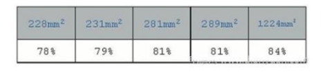
Note: The highest efficiency is 84%, and this highest efficiency is achieved when the voltage difference between input and output is low. In this case, the input/output ratio is greater than 7. In general, using two stages reduces the stage-to-stage ratio, but the efficiency obtained through two regulators is not better.
Next, we choose the highest switching frequency with the smallest PCB area. High switching frequencies are most likely to cause problems in layout. Webench then generates a circuit diagram with all active and passive components.
Circuit Design
Refer to the current path in Figure 1: the path through which the FET flows when it is on is marked in red; the loop through which the FET flows when it is off is marked in green. We observe two different situations: the area with two colors and the area with only one color. We must pay special attention to the latter case because the current alternates between zero and full-scale voltage. These are all high di/dt areas.
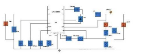
Figure 1
High di/dt AC generates a large magnetic field around the PCB traces, which is a major source of interference to other components in the circuit and even other circuits on the same or adjacent PCB. Since the common current path is assumed to be non-AC, it is not a critical path and the effect of di/dt is much smaller. On the other hand, these areas are more loaded over time. In this case, the common path is from the cathode of the diode to the output and from the output ground to the anode of the diode. The output capacitor has a very high di/dt when it charges and discharges. All the lines connecting the output capacitor must meet two conditions: they should be wide due to the high current and they should be as short as possible to minimize the di/dt effect.
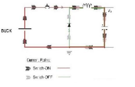
Figure 2
In fact, the designer should not use the so-called traditional layout method of leading wires from Vout and ground to the capacitor. These wires should be flowing with large AC. It is better to connect the output and ground directly to the capacitor terminals. Therefore, the alternating current is only shown on the capacitor. The other wires connecting the capacitor now flow with almost constant current and any problems related to di/dt are solved.
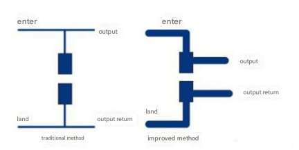
Figure 3
Ground design is another area where misunderstanding often occurs. Simply putting a ground plane on ‘level 2’ and connecting all ground connections to it will not give good results.
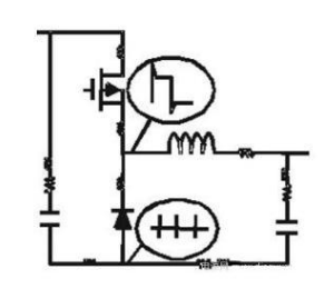
Figure 4
Let’s see why. Our design example shows that there is up to 3A of current that must flow from ground back to the source (a 24V car battery or a 24V power supply). There will be large currents in the ground connections of the diode, COUT, CIN and the load. The switching regulator ground connection flows a small current. The same situation applies to the ground reference of the resistor divider. If all the above ground pins are connected to a ground plane, we will experience ground bouncing. Although small, the inductive points in the circuit (such as the resistor divider from which the feedback voltage is obtained) will not have a stable reference ground. As a result, the overall regulation accuracy will be greatly affected. In fact, we will even get ‘ringing’ from the hidden ground plane of level 2, which is very difficult to locate.
In addition, high current connections must use vias to the ground plane, which is another source of interference and noise. It is better to use the CIN ground connection as a star node for all high current ground traces on the input and output sides of the circuit. The star node connects the ground plane and the two low current ground connections (IC and voltage divider).
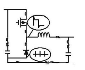
Figure 5
Now the ground plane is clean: no high currents, no ground bounce. All high current grounds are connected to the CIN ground in a star shape. All the designer must do is to make the ground traces (all on the first layer of the PCB) as short and thick as possible. In this context, saving copper will basically not get good results.
Node Impedance
High impedance nodes should be checked because they are prone to interference.
The most critical node is the feedback pin of the IC, where the signal is taken from the resistor divider. The FB pin is the input of the amplifier (such as LM25576) or the comparator (such as in the case of hysteresis regulator). In both cases, the impedance of the FB point is quite high. Therefore, the resistor divider should be placed to the right of the FB pin, and a short wire should be connected from the middle of the resistor divider to FB. The wire from the output to the resistor divider is low impedance, and a longer wire can be used to connect to the resistor divider. The focus here is on the routing method rather than the wire length.
Other nodes are not so critical. So don’t worry about the switch node, the diode, COUT, the VIN pin of the switch IC, or CIN.
Wiring Tips
The routing method will make a difference for the resistor divider. The wire runs from COUT to the resistor divider, and its ground returns to COUT. We must ensure that this loop does not form an open area. An open area will act as a receiving antenna. If we can ensure that the ground plane under the wire is free of interference, then the area formed by the wire and the ground under it and between level1 and level2 should be free of interference. Now, we can see why the ground should not be placed on level4, because the distance is significantly increased.
Another way is that the ground connection of the resistor divider can be routed to level1, making the two wires parallel and as close as possible to make the area smaller. These observations apply to all traces through which a signal flows: sensor connections, amplifier outputs, inputs to an ADC or audio power amplifier. For every analog signal, make it less susceptible to the introduction of noise.
The requirement to minimize open area whenever possible also applies to low-impedance traces; in this case, we have a potential source (antenna) of interference signals to other parts of the PCB or other devices. Note: the smaller the better when it comes to open area.
Two traces are also critical: from the IC’s switch output to the diode and inductor node; and from the diode to the node. Both of these traces have high di/dt: either the switch is on or the diode is flowing current, so the traces should be as short and thick as possible. The traces from the node to the inductor and from the inductor to COUT are less critical. In this case, the inductor current is relatively constant and changes slowly. What we want to do is make sure it is a low-impedance point to minimize voltage drops.
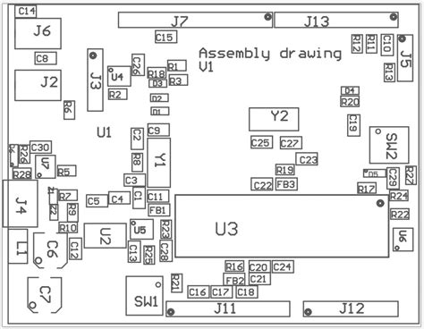
Actual Layout
Let’s take a look at a good layout (below). The main component is an MSOP-8 packaged controller used with an external FET.
Observe the space near CIN. Note: The ground point of the capacitor is directly connected to the diode anode. You cannot make the wire in the ‘power ground’ too short! The FET [SW] should be moved up a few millimeters to shorten the cathode-inductor-FET wire.
The COUT area is not visible. But we can observe that the resistor divider (FB1-FB2) is very close to the IC. FB2 is connected to another ground plane, and the ground pin of the IC is treated the same way. The ‘signal’ ground is connected to the ground plane with three vias, and the ‘power’ ground is also connected to the GND pin of the PCB with three vias. In this way, the ‘signal’ ground will not ‘see’ any ground bounce of the ‘power’ ground.
If you follow a few simple rules (only some of which are discussed in this article), you will not have trouble with your PCB layout. Thinking carefully about the PCB layout before you start will save you time and effort in dealing with anomalies in switching power supplies.