PCB Layout Considerations for Linear Power Supplies and High-Frequency Switching Power Supplies
Introduction
Printed Circuit Board (PCB) layout is a critical factor in the performance, efficiency, and reliability of both linear and switching power supplies. While these two power supply types serve similar purposes—converting and regulating electrical power—their operating principles differ significantly, leading to distinct PCB layout requirements. This 2000-word article explores the key considerations for optimizing PCB layouts for linear power supplies and high-frequency switching power supplies, highlighting their differences and specific design challenges.
Section 1: Fundamentals of Linear Power Supply PCB Layout
1.1 Characteristics of Linear Power Supplies
Linear power supplies operate by dropping excess voltage across a series pass transistor operating in its linear region. This simple operation results in several distinctive characteristics:
- Low noise output due to absence of switching
- Limited to step-down conversion
- Lower efficiency, especially with large voltage differentials
- Typically lower frequency operation compared to switchers
1.2 Key PCB Layout Considerations
Thermal Management
The most critical aspect of linear power supply layout is thermal management since the regulator dissipates power equal to (Vin – Vout) × Iload:
- Heat sink placement: Position the regulator close to the board edge or designated heat sink area
- Thermal vias: Use multiple vias under the regulator package to conduct heat to inner layers or bottom side
- Copper pours: Maximize copper area around the regulator for heat dissipation
- Component spacing: Allow adequate air flow around high-heat components
Grounding Strategy
Linear supplies are less sensitive to grounding issues than switchers but still require attention:
- Use a star ground configuration with the regulator ground as the central point
- Keep high current return paths short and wide
- Separate analog and digital grounds if the supply powers mixed-signal circuits
Component Placement
- Position filter capacitors close to the input and output pins
- Keep sensitive analog components away from potential heat sources
- Place bypass capacitors as close as possible to IC power pins
Trace Routing
- Use wide traces for high-current paths (input, output, and ground)
- Maintain adequate spacing between high-voltage traces
- Minimize loop areas in critical current paths
Section 2: High-Frequency Switching Power Supply PCB Layout
2.1 Characteristics of Switching Power Supplies
Switching power supplies operate by rapidly switching transistors between fully on and fully off states, offering several distinct characteristics:
- High efficiency across wide input/output ranges
- Capable of step-up, step-down, and inverting conversions
- High-frequency operation (typically 50kHz to several MHz)
- Electromagnetic interference (EMI) generation due to switching transitions
2.2 Key PCB Layout Considerations
Minimizing Parasitics
Switchers are extremely sensitive to parasitic inductance and capacitance:
- Minimize loop areas in high di/dt paths (switch nodes, gate drive)
- Keep high-current paths short and wide
- Place critical components (switches, diodes, inductors) close together
Thermal Management
While more efficient than linear regulators, switchers still require thermal consideration:
- Position hot components (switches, diodes) with adequate copper area
- Use thermal vias under power components
- Consider component height for possible forced air cooling
EMI Reduction Techniques
High-frequency operation generates significant EMI that must be contained:
- Proper grounding: Use a solid ground plane when possible
- Shielding: Consider shields for sensitive circuits or high-radiation components
- Filtering: Place input/output filters close to connectors
- Component placement: Keep noisy circuits away from sensitive analog sections
Critical Node Management
The switch node (connection between switch, diode, and inductor) is particularly sensitive:
- Keep this node physically small to minimize radiated EMI
- Avoid routing sensitive signals near or under the switch node
- Consider using a ground shield under the switch node in sensitive applications
Section 3: Comparative Analysis of Layout Approaches
3.1 Grounding Strategies
Linear Supplies:
- Prefer star grounding
- Can tolerate longer ground paths
- Less sensitive to ground plane cuts
Switching Supplies:
- Require low-impedance ground planes
- Sensitive to ground bounce
- May need split grounds with controlled connections
3.2 Component Placement
Linear Supplies:
- Focus on thermal placement
- Less critical component positioning (except filters)
- More forgiving of longer traces
Switching Supplies:
- Critical component placement is essential
- Must minimize parasitic inductances
- Sensitive to component orientation and proximity
3.3 Board Stackup Considerations
Linear Supplies:
- Can often use simpler 2-layer designs
- Less demanding on layer arrangement
- Fewer high-speed signals to manage
Switching Supplies:
- Often require 4+ layers for proper performance
- Need careful layer stackup planning
- Typically dedicate entire layers to ground/power planes
3.4 Thermal Design
Linear Supplies:
- Primary challenge is heat dissipation
- Large copper areas essential
- May require external heat sinks
Switching Supplies:
- Heat more distributed among components
- Focus on reducing conduction losses
- Often use internal layers for heat spreading
Section 4: Advanced Layout Techniques
4.1 Multi-layer Board Strategies
For complex designs, advanced techniques become necessary:
- Power planes: Dedicate entire layers to critical voltages
- Ground stitching: Multiple vias connect ground layers
- Impedance control: Important for gate drive signals in switchers
4.2 High-Current Routing
Both supply types may need to handle substantial currents:
- Copper thickness: Specify appropriate oz/ft² copper weight
- Exposed copper: Use solder mask openings to increase current capacity
- Bus bars: Consider for very high current applications
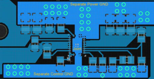
4.3 Mixed-Signal Considerations
When power supplies serve analog and digital circuits:
- Ground separation: May need split analog/digital grounds
- Supply filtering: Additional filtering for sensitive circuits
- Noise isolation: Physical separation of noisy and quiet circuits
Section 5: Practical Design Examples
5.1 Linear Regulator Layout Example
A 5V, 1A linear regulator from 12V input:
- Place regulator near board edge for heat sinking
- 1000µF bulk input capacitor within 10mm of input pin
- 10µF ceramic output capacitor adjacent to output pin
- Wide traces (100mil+) for input/output/ground
- Thermal relief for all pad connections
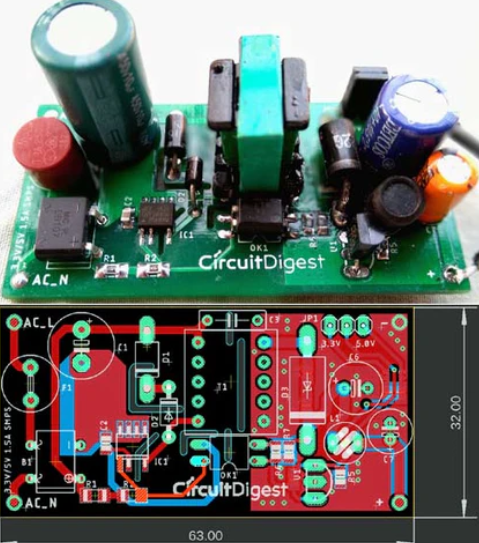
5.2 Buck Converter Layout Example
A 500kHz, 12V to 5V buck converter:
- Tight placement of MOSFET, diode, inductor, and controller
- Smallest possible switch node area
- Ground plane on adjacent layer
- Input capacitors close to MOSFET drain
- Output capacitors near inductor
- Separate analog and power grounds, joined at IC
Section 6: Common Layout Mistakes to Avoid
6.1 Linear Supply Pitfalls
- Inadequate heat sinking
- Excessive trace lengths for filter capacitors
- Poor grounding of adjustment pins
- Underestimating required copper area
6.2 Switching Supply Pitfalls
- Large high-di/dt loops
- Poor placement of input/output filters
- Inadequate attention to switch node
- Improper gate drive routing
- Ground plane splits that increase impedance
Section 7: Verification and Testing
7.1 Design Rule Checks (DRC)
- Verify spacing rules for high-voltage sections
- Check thermal relief settings
- Confirm adequate trace widths
7.2 Signal Integrity Analysis
For switching supplies particularly:
- Simulate critical nets for ringing/overshoot
- Verify gate drive signal quality
- Check for unintended coupling
7.3 Thermal Analysis
- Estimate component temperatures
- Verify heat sinking adequacy
- Identify potential hot spots
Conclusion
Effective PCB layout is essential for realizing the full performance potential of both linear and switching power supplies. While linear supplies primarily demand careful thermal design and straightforward routing, switching supplies require meticulous attention to high-frequency current paths, EMI control, and minimization of parasitic elements. By understanding and applying the distinct layout requirements for each power supply type, designers can create reliable, efficient power conversion circuits that meet their application requirements. As power supply designs continue to evolve with higher frequencies and greater power densities, PCB layout will remain a critical factor in successful power system design.