PCB layout, electromagnetic compatibility analysis (EMC), power integrity analysis
Regarding the issue of PCB layout and routing, today we will not talk about signal integrity analysis (SI), electromagnetic compatibility analysis (EMC), and power integrity analysis (PI). We will only talk about manufacturability analysis (DFM). Unreasonable manufacturability design will also lead to product design failure.
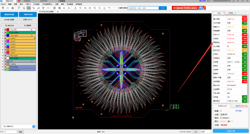
Successful DFM in PCB layout begins with setting design rules to consider important DFM constraints. The DFM rules shown below reflect some contemporary design capabilities that can be found in most manufacturers. Make sure that the restrictions set in the PCB design rules do not violate these restrictions so that most standard design restrictions can be ensured.
The DFM problem of PCB routing depends on good PCB layout. The routing rules can be set in advance, including the number of bends of the routing, the number of vias, the number of steps, etc. Generally, exploratory routing is performed first to quickly connect the short lines, and then maze routing is performed. The global routing path optimization of the connection to be routed is first performed, and try to re-route to improve the overall effect and DFM manufacturability issues.
01DFM of PCB layout
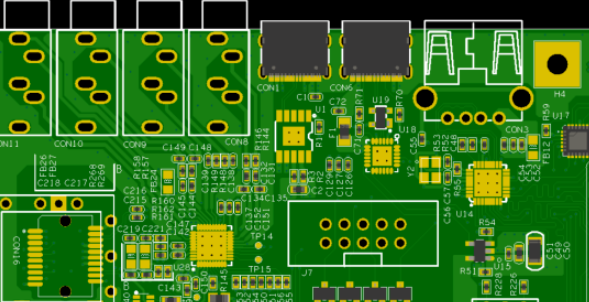
1.SMT devices
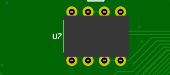
The device layout spacing meets the assembly requirements. Generally, the surface mount devices are greater than 20mil, the IC type is greater than 80mil, and the BGA type is greater than 200mi. The device spacing during layout meets the assembly requirements to improve the quality yield of the production process.
The device pin SMD pad spacing generally needs to be greater than 6mil, and the solder mask bridge manufacturing capacity is 4mil. If the SMD pad spacing is less than 6mil, the solder mask window spacing is less than 4mil, and the solder mask bridge cannot be retained, resulting in large pieces of solder (especially between pins) during assembly, which leads to short circuits.

2.DIP devices
The device pin spacing, device direction, and device spacing of devices processed by wave soldering must take into account the requirements of wave soldering processing. Insufficient device pin spacing will cause soldering to connect, which will lead to short circuits.
Many designers will minimize the use of through-hole devices (THT) or place through-hole devices on the same side of the board. However, through-hole devices are often unavoidable. In the case of combination, if the through-hole device is placed on the top layer and the surface-mount device is placed on the bottom layer, in some cases, it will affect the single-sided wave soldering. At this time, a more expensive welding process, such as selective welding, should be used.
3.The distance between components and the edge of the board
If it is welded on the machine, the distance between the electronic components and the edge of the board is generally 7mm (different welding manufacturers have different requirements), but it is also possible to add a process edge when making the PCB, so that the electronic components can be placed on the edge of the PCB board, as long as it is convenient for wiring.
However, when the device on the edge of the board is welded by the machine, it may touch the guide rail of the machine and damage the components. The device pads on the edge of the board will be cut off during the manufacturing process. If the pads are relatively small, it will affect the welding quality.
4.The distance between high/low devices
There are many types of electronic components, different shapes, and various lead wires, so the assembly methods of printed circuit boards are also different. A good layout can not only make the machine performance stable, shockproof, and reduce damage, but also get a neat and beautiful effect inside the machine.
Around the high device, the short device needs to keep a certain distance. The device distance is small compared to the device height, and there is uneven heat wave, which may cause poor welding or the risk of being unable to repair after welding.
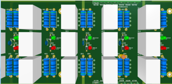
5.Spacing between devices
In general, when mounting chips in SMT processing, it is necessary to consider that there are certain errors in machine mounting, and to facilitate maintenance and visual appearance inspection. The adjacent components should not be too close, and a certain safety distance should be left.
The spacing between chip components, between SOTs, and between SOIC and chip components is 1.25mm. The spacing between chip components, between SOTs, and between SOIC and chip components is 1.25mm. The spacing between PLCC and chip components, SOIC, and QFP is 2.5mm. The spacing between PLCC is 4mm. When designing a PLCC socket, pay attention to the size of the PLCC socket (the pins of the PLCC are on the bottom inner side of the socket).
02.DFM of PCB wiring:
1.Line width/line spacing
For designers, we cannot only consider the precision and perfection requirements of the design during the design process. Another major constraint is the problem of production process. It is impossible for a board factory to rebuild a production line for the birth of an excellent product.
Under normal circumstances, the line width and line spacing are controlled to 4/4mil, and the via is selected to be 8mil (0.2mm). Basically, more than 80% of PCB manufacturers can produce it, and the production cost is the lowest. The minimum line width and line spacing is controlled to 3/3mil, and the via is selected to be 6mil (0.15mm). Basically, more than 70% of PCB manufacturers can produce it, but the price is slightly more expensive than the first case, not much more expensive.
2.Sharp angle/right angle
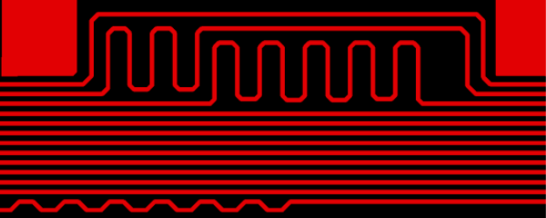
Sharp angle routing is generally prohibited during wiring. Right angle routing is generally required to be avoided as much as possible in PCB wiring, and it has almost become one of the standards for measuring the quality of wiring. Because it affects the integrity of the signal, right angle routing will generate additional parasitic capacitance and parasitic inductance.
In the PCB plate making process, the intersection of PCB wires to form a sharp angle will cause a problem called acid angle. In the PCB line etching process, the “acid angle” will cause excessive corrosion of the PCB line, resulting in the problem of virtual disconnection of the PCB line. Therefore, PCB engineers need to avoid sharp or strange angles in the traces, and the traces should be kept at a 45-degree angle at the bends.
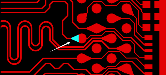
3.Copper strips/islands
If the island copper is large enough, it will become an antenna, which may cause noise and other interference within the circuit board (because its copper is not grounded – it will become a signal collector).
Copper strips and islands are free-floating copper on many plane layers, which can cause some serious problems in the acid tank. It is well known that small copper spots will fall off the PCB panel and reach other etched areas on the panel, causing short circuits.
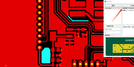
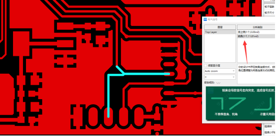
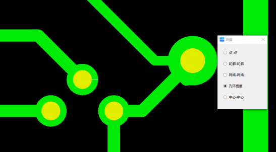
4.Drilled hole ring
The hole ring refers to a circle of copper around the drill hole. Due to tolerances in the manufacturing process, after drilling, etching, and copper plating, the remaining copper ring around the drill hole, the drill bit does not always perfectly hit the center point of the pad, so the hole ring may break.
The hole ring of the via needs to be larger than 3.5mil on one side, and the plug-in hole ring is larger than 6mil. The hole ring is too small. During the manufacturing process, there is a tolerance for drilling and alignment of the lines. The deviation of the tolerance will cause the hole ring to break and open the circuit.
5.Teardrops for wiring
Adding teardrops to PCB wiring can make the connection of the circuit on the PCB board more stable and reliable, so that the system will be more stable, so it is necessary to add teardrops to the circuit board.
Adding teardrops can prevent the contact point between the wire and the pad or the wire and the guide hole from being disconnected when the circuit board is hit by a huge external force. When adding teardrops for welding, the pad can be protected to avoid multiple welding and the pad falling off. During production, uneven etching and cracks caused by the deviation of the via can be avoided.
DFM detection layout and wiring