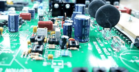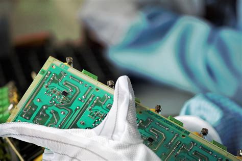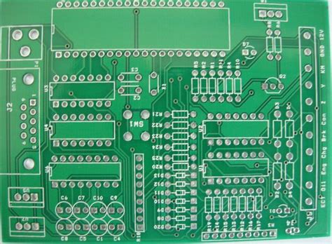
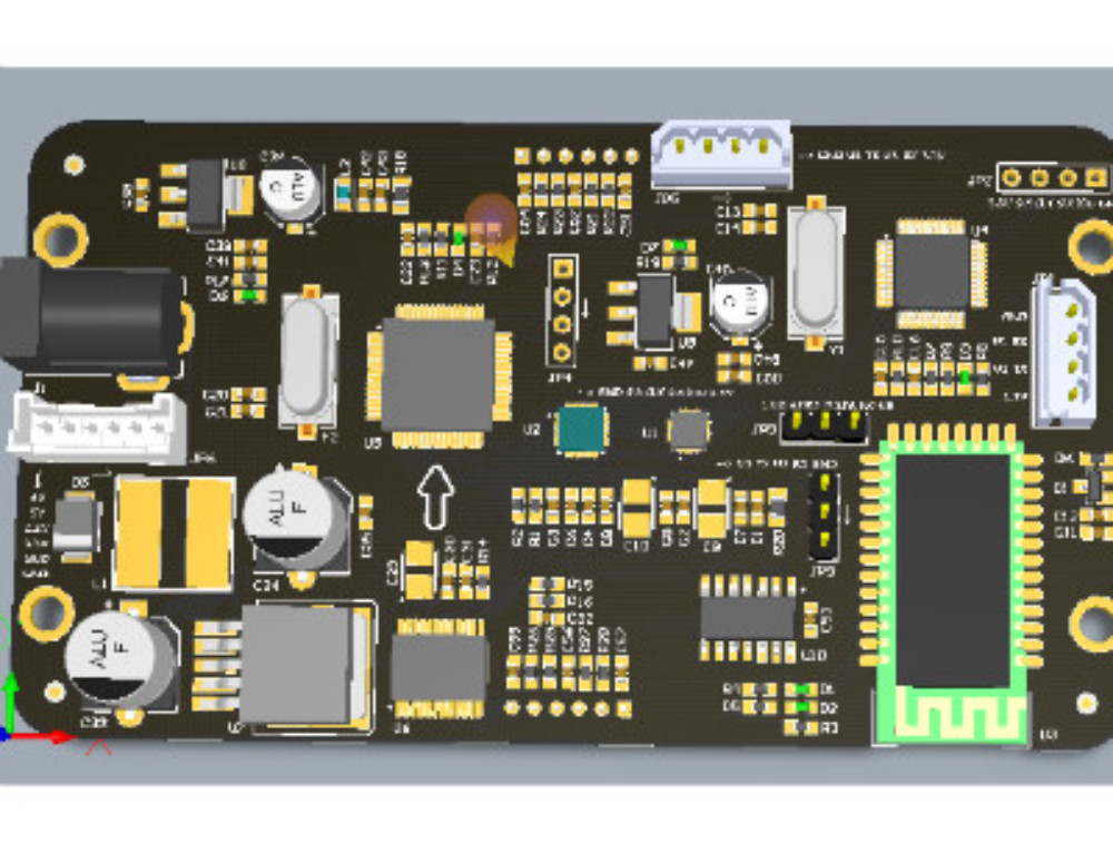
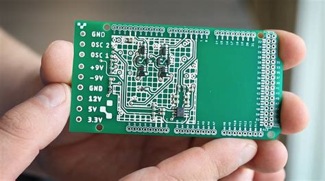
Pcb layout high speed test points
Optimizing Test Point Placement for High-Speed PCB Layouts
In the realm of high-speed printed circuit board (PCB) design, the strategic placement of test points is paramount to ensuring both the functionality and reliability of the final product. As electronic devices continue to evolve, the demand for higher data rates and faster signal processing has necessitated meticulous attention to every aspect of PCB layout. Test points, which serve as designated locations for probing and measuring electrical signals, play a crucial role in the validation and debugging processes. Therefore, optimizing their placement is essential for maintaining signal integrity and achieving accurate test results.
To begin with, it is important to understand that high-speed signals are particularly susceptible to various forms of interference and signal degradation.
Factors such as crosstalk, electromagnetic interference (EMI), and signal reflection can significantly impact the performance of high-speed circuits. Consequently, the placement of test points must be carefully considered to minimize these adverse effects. One effective strategy is to position test points in areas where the signal path is least likely to be disrupted. This often involves placing them at the end of transmission lines or at key nodes within the circuit where critical measurements are required.
Moreover, the physical characteristics of the test points themselves can influence signal integrity.
For instance, the size and shape of the test pads, as well as the type of probe used, can introduce parasitic capacitance and inductance. These parasitic elements can alter the impedance of the signal path, leading to potential signal distortion. To mitigate these issues, designers should opt for test points that are as small as possible while still being accessible for probing. Additionally, using high-impedance probes can help minimize the loading effect on the circuit, thereby preserving the integrity of the measured signals.
Transitioning to the layout considerations, it is essential to maintain a consistent ground reference for all test points.
A stable ground plane helps reduce noise and provides a common reference point for measurements. When placing test points, designers should ensure that they are connected to a solid ground plane with minimal interruptions. This can be achieved by avoiding ground plane splits and ensuring that the ground connections are as short and direct as possible. Furthermore, placing decoupling capacitors near test points can help filter out high-frequency noise, further enhancing measurement accuracy.
Another critical aspect of test point placement is accessibility.
During the testing phase, engineers need to be able to easily access the test points without causing damage to the PCB or other components. This requires careful planning during the layout stage to ensure that test points are not obstructed by other components or located in areas that are difficult to reach. Additionally, providing clear labeling and documentation for each test point can facilitate the testing process and reduce the likelihood of errors.
In conclusion, optimizing test point placement for high-speed PCB layouts is a multifaceted challenge that requires careful consideration of signal integrity, physical characteristics, ground referencing, and accessibility. By strategically positioning test points and employing best practices in PCB design, engineers can ensure accurate and reliable measurements, ultimately leading to the successful validation and performance of high-speed electronic devices. As technology continues to advance, the importance of meticulous test point placement will only grow, underscoring the need for ongoing innovation and attention to detail in PCB design.

Best Practices for High-Speed PCB Test Point Design
Designing test points for high-speed printed circuit boards (PCBs) is a critical aspect of ensuring the reliability and performance of electronic devices. As the demand for faster and more efficient electronic systems continues to grow, the need for meticulous attention to detail in PCB layout becomes increasingly important. To achieve optimal results, it is essential to adhere to best practices that address the unique challenges posed by high-speed signals.
One of the primary considerations in high-speed PCB test point design is signal integrity.
High-speed signals are susceptible to various forms of interference, such as crosstalk, electromagnetic interference (EMI), and signal reflection. To mitigate these issues, it is crucial to place test points strategically. Ideally, test points should be located in areas where they cause minimal disruption to the signal path. This often means placing them at the end of a trace or in a location where the signal has already been conditioned.
Moreover, the physical design of the test points themselves plays a significant role in maintaining signal integrity.
Test points should be as small as possible to reduce their impact on the signal. However, they must also be large enough to allow for reliable probing. A balance must be struck between minimizing the test point size and ensuring that it is accessible for testing equipment. Additionally, the use of vias should be minimized, as they can introduce unwanted inductance and capacitance, which can degrade signal quality.
Another important aspect of high-speed PCB test point design is the consideration of impedance matching.
Impedance mismatches can lead to signal reflections, which can cause data corruption and signal degradation. To avoid this, test points should be designed to match the impedance of the signal trace as closely as possible. This can be achieved by carefully controlling the geometry of the test point and the surrounding traces. For instance, maintaining consistent trace width and spacing can help ensure that the impedance remains uniform.
Thermal management is also a critical factor in high-speed PCB design.
High-speed signals can generate significant amounts of heat, which can affect the performance and reliability of the PCB. Test points should be designed with thermal considerations in mind, ensuring that they do not contribute to excessive heat buildup. This can be achieved by using thermal reliefs and ensuring adequate spacing between test points and other heat-sensitive components.
Furthermore, the choice of materials used in the PCB can have a significant impact on high-speed signal performance.
High-frequency laminates with low dielectric constants and low loss tangents are preferred for high-speed applications. These materials help to minimize signal loss and maintain signal integrity. When designing test points, it is important to ensure that the materials used are compatible with the overall PCB design and do not introduce additional signal degradation.
In addition to these technical considerations, it is also important to consider the practical aspects of testing.
Test points should be easily accessible for probing, and their locations should be clearly documented in the design files. This facilitates efficient testing and troubleshooting, reducing the time and effort required to verify the PCB’s performance.
In conclusion, designing test points for high-speed PCBs requires a careful balance of technical and practical considerations. By focusing on signal integrity, impedance matching, thermal management, material selection, and accessibility, designers can ensure that their high-speed PCBs perform reliably and efficiently. Adhering to these best practices will help to minimize signal degradation and interference, ultimately leading to more robust and high-performing electronic systems.
Challenges in High-Speed PCB Layouts: Test Points and Signal Integrity
In the realm of high-speed printed circuit board (PCB) design, ensuring signal integrity and incorporating effective test points present significant challenges. As electronic devices become increasingly sophisticated, the demand for high-speed data transmission grows, necessitating meticulous attention to PCB layout. One of the critical aspects of this process is the strategic placement of test points, which are essential for debugging, testing, and validating the performance of the PCB. However, the integration of these test points must be carefully managed to avoid compromising signal integrity.
Signal integrity is paramount in high-speed PCB designs, as any degradation can lead to data corruption, increased error rates, and overall system instability.
High-speed signals are particularly susceptible to issues such as crosstalk, electromagnetic interference (EMI), and signal reflection. These phenomena can distort the signal waveform, making it difficult to achieve reliable communication between components. Therefore, maintaining signal integrity requires a comprehensive understanding of the electrical characteristics of the PCB and the behavior of high-speed signals.
One of the primary challenges in high-speed PCB layouts is the placement of test points without introducing additional noise or signal degradation.
Test points are used to probe signals during the testing phase, allowing engineers to verify the functionality and performance of the circuit. However, adding test points can create discontinuities in the signal path, leading to impedance mismatches and reflections. To mitigate these issues, designers must carefully consider the location and design of test points, ensuring they do not interfere with the high-speed signal traces.
To address these challenges, designers often employ several strategies.
One approach is to use surface-mount test points, which have a smaller footprint and can be placed closer to the signal traces without causing significant disruption. Additionally, designers can use via-in-pad technology, where the test point is integrated into the pad of a surface-mount component. This technique minimizes the impact on signal integrity by reducing the length of the signal path discontinuity.
Another important consideration is the use of controlled impedance traces.
High-speed signals require traces with specific impedance values to minimize reflections and ensure signal integrity. When adding test points, designers must ensure that the impedance of the trace remains consistent. This can be achieved by carefully designing the test point and its surrounding area to match the impedance of the signal trace. Furthermore, designers can use simulation tools to model the impact of test points on signal integrity, allowing them to make informed decisions about their placement and design.
In addition to these strategies, designers must also consider the impact of test points on EMI.
High-speed signals can generate significant electromagnetic radiation, which can interfere with other components and systems. To minimize EMI, designers can use shielding techniques, such as ground planes and guard traces, to isolate high-speed signals from sensitive areas of the PCB. Additionally, careful routing of signal traces and test points can help reduce the potential for EMI.
In conclusion, the integration of test points in high-speed PCB layouts presents a complex challenge that requires careful consideration of signal integrity and EMI. By employing strategies such as surface-mount test points, via-in-pad technology, controlled impedance traces, and shielding techniques, designers can effectively incorporate test points without compromising the performance of the PCB. As electronic devices continue to evolve, the importance of maintaining signal integrity in high-speed designs will only grow, making the careful management of test points an essential aspect of modern PCB design.
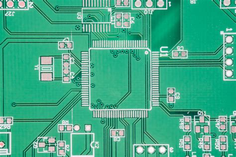
Advanced Techniques for High-Speed PCB Test Point Integration
In the realm of high-speed printed circuit board (PCB) design, the integration of test points is a critical aspect that demands meticulous attention. As electronic devices continue to evolve, the need for precise and reliable testing methods becomes increasingly paramount. Test points serve as crucial nodes for monitoring and diagnosing the performance of high-speed circuits, ensuring that the final product meets stringent quality standards. Advanced techniques for integrating these test points can significantly enhance the accuracy and efficiency of the testing process.
One of the foremost considerations in high-speed PCB test point integration is the placement of these points.
Strategic placement is essential to minimize signal degradation and maintain the integrity of high-speed signals. It is imperative to position test points in locations that provide easy access for probes while avoiding areas that could introduce noise or interference. This often involves a careful balance between accessibility and signal integrity, necessitating a thorough understanding of the PCB’s layout and the behavior of high-speed signals.
Moreover, the choice of test point types plays a pivotal role in the overall effectiveness of the testing process.
There are various types of test points, including through-hole, surface-mount, and pad-style test points, each with its own set of advantages and limitations. Through-hole test points, for instance, offer robust mechanical stability but may introduce unwanted inductance at high frequencies. Surface-mount test points, on the other hand, are more suitable for high-speed applications due to their lower inductance and smaller footprint. Selecting the appropriate type of test point is crucial to ensuring accurate measurements and reliable performance.
In addition to placement and type selection, the design of the test point itself must be optimized for high-speed applications.
This involves minimizing parasitic capacitance and inductance, which can distort high-speed signals and lead to erroneous test results. Techniques such as using short and wide traces, maintaining consistent trace impedance, and avoiding sharp corners can help mitigate these issues. Furthermore, incorporating ground planes and shielding can provide additional protection against electromagnetic interference (EMI), further enhancing the reliability of the test points.
Another advanced technique involves the use of differential test points for high-speed differential signals.
Differential signaling is commonly used in high-speed circuits to reduce noise and improve signal integrity. By incorporating differential test points, designers can accurately measure the performance of differential pairs without introducing common-mode noise. This requires careful matching of the test point pairs and maintaining consistent trace geometry to ensure accurate differential measurements.
Furthermore, the integration of automated test equipment (ATE) can streamline the testing process and improve efficiency.
ATE systems can be programmed to perform a wide range of tests, from basic continuity checks to complex signal integrity analyses. By incorporating test points that are compatible with ATE systems, designers can facilitate automated testing and reduce the likelihood of human error. This not only speeds up the testing process but also enhances the overall reliability and accuracy of the results.
In conclusion, the integration of high-speed PCB test points is a multifaceted process that requires careful consideration of placement, type selection, design optimization, and compatibility with automated testing systems. By employing advanced techniques and maintaining a keen focus on signal integrity, designers can ensure that their high-speed circuits are thoroughly tested and meet the highest standards of performance and reliability. As technology continues to advance, the importance of precise and reliable test point integration will only grow, underscoring the need for ongoing innovation and expertise in this critical area of PCB design.