PCB Layout Tutorial
Designing a printed circuit board (PCB) is the delicate process of turning a circuit schematic into a real application. You need to consider many factors in a real circuit that will affect your results almost as much as the quality of your schematic.
Unlike theoretical components, real-world devices generate heat, wires and traces have inherent resistance, and traces that run too close together can become capacitors or create shorts due to manufacturing defects. A well-designed PCB will be easy to assemble; have a clear and logical flow; and avoid electrical problems.
Instructions
- Open your PCB layout software and create a new project file. Set the board size to the specifications of your project and enable the “Snap to Grid” feature in the software. “Snap to Grid” is a standard feature of PCB layout software and will make it easier to place components in order.
- Place components that need to have specific locations first. This includes mounting holes, switches, LEDs, heat sinks, or any other component that will be connected to the outside or mounted on a cabinet.
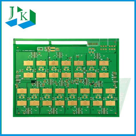
- Separate components into functional groups to make the layout more logical and understandable. For example, separate logic and input/output sections into different groups. Place all power components in one area of the board, and separate digital and analog components. High-frequency digital signals can create interference in analog circuits.
- Place all polarized components in the same orientation, and place ICs in the same way so that pin 1 is in the same place on each chip. This will make placing components much easier and help you avoid mistakes when you actually put the board together.
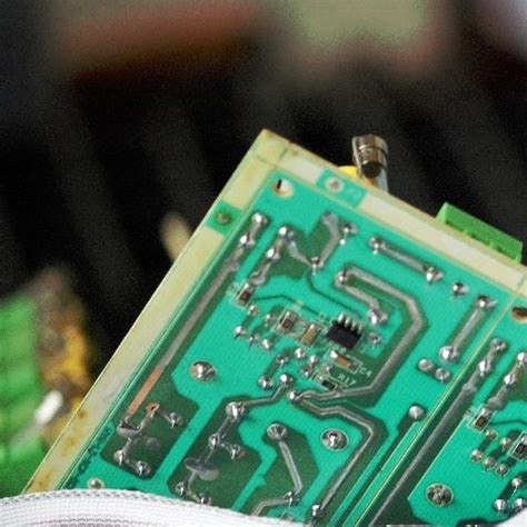
- Connect components together to minimize trace lengths. Short traces are easier to route and help you avoid trouble with noise, inherent resistance, and board capacitance. Power filter capacitors should be placed very close to the IC pins they are connected to. Every component should be placed on the top of the board unless there is absolutely no way to avoid placing some components on the bottom.
- Set trace widths based on the amount of current you expect them to carry. High-current lines need wider traces; 0.01-inch is a good width for low-power digital and analog signals of around 0.3 amps and less. 0.7-amp signals should use 0.02-inch-wide traces, while 1-amp signals should use 0.025-inch-wide traces. When a trace must be rotated, use a pair of 45-degree angles instead of a sharp 90-degree angle to avoid noise generation and prevent manufacturing defects. Use vias, which are holes that go through from one layer of the board to another, for traces that must cross without a connection.
- After placing the components, place the power and ground rails. Make your power rail a single wide trace that can branch out as needed, rather than having a bunch of traces coming off the power supply or daisy-chaining the supplies together. Also make a large, solid ground plane. Good grounding is critical and helps minimize noise.
- Simulate heat dissipation on your board if your software has this capability. Keep heat-generating components (like transformers) away from heat-sensitive components (like ICs), and place heat sinks if necessary.