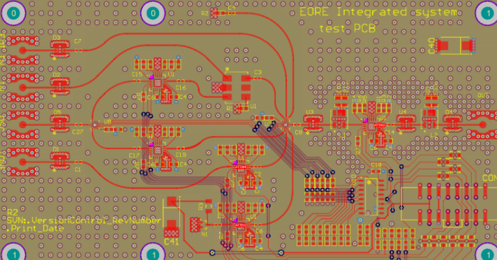
Pcb layouting
Optimizing Test Point Placement for High-Speed PCB Layouts
In the realm of high-speed printed circuit board (PCB) design, the strategic placement of test points is a critical factor that can significantly influence the performance and reliability of the final product.
As electronic devices continue to evolve, the demand for higher data rates and faster signal processing has necessitated meticulous attention to every aspect of PCB layout, including the optimization of test points. This process involves a delicate balance between ensuring accessibility for testing and maintaining the integrity of high-speed signals.
To begin with, it is essential to understand that high-speed signals are highly susceptible to noise and interference.
Therefore, the placement of test points must be carefully considered to avoid any adverse effects on signal integrity. One of the primary considerations is the minimization of signal path disruption. Test points should be placed in locations where they do not introduce significant impedance discontinuities, which can lead to signal reflections and degradation. This often means positioning test points at locations where the signal path is least likely to be affected, such as at the end of a transmission line or at a via.
Moreover, the physical size and shape of the test points themselves can impact high-speed performance.
Test points that are too large can create parasitic capacitance and inductance, which can alter the signal characteristics. Therefore, it is advisable to use test points that are as small as possible while still being functional for testing purposes. Additionally, the use of surface-mount test points can help reduce the impact on signal integrity compared to through-hole test points, as they introduce less disruption to the signal path.
Transitioning to the topic of accessibility, it is crucial to ensure that test points are placed in locations that are easily accessible for testing equipment.
This often requires a compromise between optimal signal integrity and practical accessibility. For instance, placing test points on the top or bottom layers of the PCB can facilitate easier access during testing, but it may also expose the test points to potential sources of noise. To mitigate this, designers can use shielding techniques or place test points in less noise-prone areas of the PCB.
Furthermore, the use of differential pairs in high-speed designs adds another layer of complexity to test point placement.
Differential signals require careful matching of trace lengths and impedance to maintain signal integrity. When adding test points to differential pairs, it is imperative to ensure that both traces are equally affected to preserve the balance of the differential signal. This often involves placing test points symmetrically and using identical test point structures for both traces.
In addition to these considerations, it is also important to account for the potential impact of test points on the overall PCB layout.
The addition of test points can complicate routing and may require additional layers or vias, which can increase the cost and complexity of the PCB. Therefore, designers must weigh the benefits of test point accessibility against the potential drawbacks in terms of layout complexity and cost.
In conclusion, optimizing test point placement for high-speed PCB layouts is a multifaceted challenge that requires careful consideration of signal integrity, accessibility, and overall layout impact. By strategically placing test points to minimize disruption to high-speed signals, using appropriately sized and shaped test points, and ensuring accessibility for testing equipment, designers can achieve a balance that supports both effective testing and optimal performance. As high-speed electronic devices continue to advance, the importance of meticulous test point placement in PCB design will only continue to grow.
Best Practices for High-Speed Signal Integrity in PCB Test Points
Ensuring high-speed signal integrity in PCB test points is a critical aspect of modern electronic design. As devices become more complex and operate at higher frequencies, maintaining signal integrity becomes increasingly challenging. To address these challenges, designers must adhere to best practices that mitigate potential issues and ensure reliable performance.
One of the primary considerations in high-speed PCB design is the placement of test points.
Test points are essential for debugging and validating the functionality of a circuit, but their placement can significantly impact signal integrity. To minimize disruptions, test points should be strategically placed along the signal path. This placement should be as close as possible to the components being tested, thereby reducing the length of the signal path and minimizing potential interference.
Moreover, the physical characteristics of the test points themselves can influence signal integrity.
It is advisable to use test points with minimal parasitic inductance and capacitance. These parasitic elements can distort high-speed signals, leading to erroneous readings and degraded performance. By selecting test points designed for high-frequency applications, designers can mitigate these adverse effects.
Another crucial factor is the routing of high-speed signals.
Proper routing techniques are essential to maintain signal integrity. For instance, differential pairs should be routed together with consistent spacing to ensure that they are subject to the same electromagnetic environment. This practice helps to maintain the integrity of the differential signal and reduces the likelihood of crosstalk and noise.
In addition to routing, the use of ground planes is vital in high-speed PCB design.
Ground planes provide a low-impedance return path for signals, which is essential for maintaining signal integrity. When placing test points, it is important to ensure that they have a solid connection to the ground plane. This connection helps to minimize ground bounce and other noise-related issues that can affect high-speed signals.
Furthermore, impedance matching is a key consideration in high-speed PCB design.
Mismatched impedance can cause signal reflections, which degrade signal integrity. To avoid this, designers should ensure that the impedance of the test points matches the impedance of the signal traces. This matching can be achieved through careful design and the use of appropriate materials and geometries.
The use of decoupling capacitors is another best practice for maintaining high-speed signal integrity.
Decoupling capacitors help to filter out noise and provide a stable power supply to the components. When placing test points, it is important to ensure that decoupling capacitors are located nearby. This proximity helps to maintain a clean power supply and reduces the likelihood of noise affecting the test points.
Additionally, signal integrity can be enhanced by minimizing the number of vias in high-speed signal paths.
Vias introduce inductance and capacitance, which can distort high-speed signals. When test points are required, it is best to place them in locations that minimize the need for vias. If vias are unavoidable, their impact can be mitigated by using techniques such as back-drilling to remove unused portions of the via.
Finally, simulation and testing are indispensable tools in ensuring high-speed signal integrity.
Before finalizing the PCB design, it is essential to use simulation tools to model the behavior of high-speed signals and identify potential issues. Once the PCB is fabricated, thorough testing should be conducted to validate the performance of the test points and ensure that signal integrity is maintained.
In conclusion, maintaining high-speed signal integrity in PCB test points requires careful consideration of placement, physical characteristics, routing, grounding, impedance matching, decoupling, and via management. By adhering to these best practices, designers can ensure reliable performance and accurate testing of high-speed circuits.
Challenges and Solutions in High-Speed PCB Test Point Design
Designing test points for high-speed printed circuit boards (PCBs) presents a unique set of challenges that require careful consideration and innovative solutions. As electronic devices continue to evolve, the demand for higher speeds and greater functionality has led to increasingly complex PCB designs. This complexity, in turn, necessitates meticulous planning and execution to ensure that test points do not compromise the performance and integrity of the high-speed signals.
One of the primary challenges in high-speed PCB test point design is maintaining signal integrity.
High-speed signals are particularly susceptible to noise, crosstalk, and signal degradation, which can be exacerbated by poorly designed test points. To mitigate these issues, designers must ensure that test points are strategically placed and properly shielded. This often involves using differential pairs and controlled impedance traces to minimize signal reflections and maintain the integrity of the high-speed signals.
Another significant challenge is the physical space constraints on the PCB.
As devices become more compact, the available real estate for placing test points becomes increasingly limited. Designers must balance the need for sufficient test points to facilitate thorough testing with the need to conserve space for other critical components. This often requires innovative solutions, such as using via-in-pad technology or embedding test points within the PCB layers, to maximize the use of available space without compromising the board’s functionality.
Thermal management is also a critical consideration in high-speed PCB test point design.
High-speed circuits generate more heat, which can affect the performance and reliability of the test points. Effective thermal management strategies, such as using thermal vias, heat sinks, and proper trace routing, are essential to dissipate heat and prevent thermal-related issues. Additionally, designers must consider the thermal expansion and contraction of materials, which can impact the mechanical stability of the test points over time.
The choice of materials and components is another crucial factor in high-speed PCB test point design.
High-frequency signals require materials with low dielectric constants and low loss tangents to minimize signal attenuation and distortion. Furthermore, the selection of connectors and probes for test points must be compatible with high-speed signals to ensure accurate measurements. This often involves using high-quality, low-inductance connectors and probes that can handle the high frequencies without introducing significant parasitic effects.
To address these challenges, designers can employ various simulation and modeling tools to predict and analyze the behavior of high-speed signals in the presence of test points.
These tools can help identify potential issues, such as signal reflections, crosstalk, and impedance mismatches, allowing designers to make informed decisions and optimize the placement and design of test points. Additionally, iterative prototyping and testing can provide valuable insights and feedback, enabling designers to refine their designs and achieve the desired performance.
In conclusion, designing test points for high-speed PCBs is a complex and multifaceted task that requires careful consideration of signal integrity, space constraints, thermal management, and material selection. By employing strategic design practices, leveraging advanced simulation tools, and iterating through prototyping and testing, designers can overcome these challenges and create high-speed PCBs with reliable and effective test points. As technology continues to advance, the importance of innovative and meticulous test point design will only grow, underscoring the need for ongoing research and development in this critical area of PCB design.

Advanced Techniques for High-Speed PCB Test Point Validation
In the realm of high-speed printed circuit board (PCB) design, the validation of test points is a critical aspect that ensures the reliability and performance of the final product. As electronic devices continue to evolve, the demand for higher data rates and faster signal processing has necessitated advanced techniques for high-speed PCB test point validation. This article delves into these sophisticated methods, providing insights into how engineers can effectively validate test points in high-speed PCB layouts.
To begin with, it is essential to understand the significance of test points in PCB design.
Test points are designated locations on a PCB where probes can be attached to measure electrical signals. These points are crucial for debugging, testing, and validating the functionality of the circuit. In high-speed designs, where signal integrity and timing are paramount, the placement and validation of test points become even more critical.
One advanced technique for high-speed PCB test point validation is the use of simulation tools.
Simulation allows engineers to model the behavior of the PCB under various conditions and identify potential issues before physical prototypes are built. By simulating the signal paths and analyzing the results, engineers can determine the optimal placement of test points to minimize signal degradation and ensure accurate measurements. This proactive approach not only saves time but also reduces the cost associated with iterative prototyping.
Another important aspect of high-speed PCB test point validation is the consideration of signal integrity.
High-speed signals are susceptible to various forms of interference, such as crosstalk, reflection, and electromagnetic interference (EMI). To mitigate these issues, engineers must carefully design the test points and their surrounding traces. For instance, maintaining proper spacing between test points and high-speed traces can help reduce crosstalk. Additionally, using controlled impedance traces and incorporating ground planes can enhance signal integrity and provide a stable reference for measurements.
Transitioning to the practical implementation, the use of advanced probing techniques is also vital for high-speed PCB test point validation.
Traditional probes may not be suitable for high-speed signals due to their inherent parasitic capacitance and inductance. Instead, engineers can employ specialized high-speed probes that are designed to minimize these parasitic effects. These probes often feature low capacitance tips and high bandwidth, enabling accurate measurements of high-speed signals without significantly loading the circuit.
Furthermore, the integration of automated test equipment (ATE) can streamline the validation process.
ATE systems are capable of performing complex test sequences and capturing high-speed data with precision. By automating the testing process, engineers can achieve consistent and repeatable results, which are essential for validating high-speed PCB designs. Additionally, ATE systems can be programmed to perform various tests, such as time-domain reflectometry (TDR) and vector network analysis (VNA), providing comprehensive insights into the performance of the test points.
In conclusion, the validation of test points in high-speed PCB layouts requires a combination of advanced techniques and careful consideration of signal integrity. Simulation tools, proper design practices, specialized probing techniques, and automated test equipment all play a crucial role in ensuring accurate and reliable measurements. As the demand for high-speed electronic devices continues to grow, these advanced techniques will become increasingly important in the quest for optimal PCB performance. By leveraging these methods, engineers can confidently validate their high-speed PCB designs, paving the way for the next generation of electronic innovations.