PCB Line Width and Spacing: A Comprehensive Guide
Introduction
Printed Circuit Board (PCB) design is a complex process that requires careful consideration of numerous factors to ensure optimal performance, reliability, and manufacturability. Among these critical factors, line width and spacing stand out as fundamental parameters that directly impact a PCB’s electrical characteristics, thermal management, signal integrity, and manufacturing yield. This 2000-word article provides an in-depth exploration of PCB line width and spacing, covering their importance, calculation methods, design considerations, and industry standards.
Understanding PCB Line Width and Spacing
Definition of Terms
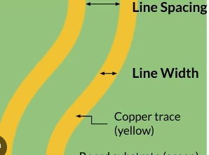
Line width refers to the width of the copper traces that form the conductive pathways on a PCB. These traces carry electrical signals and power between components. Line width is typically measured in mils (thousandths of an inch) or millimeters.
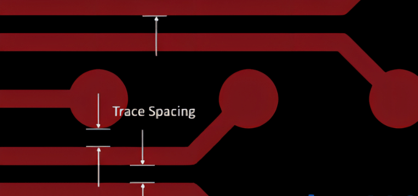
Spacing (also called clearance or track-to-track distance) is the distance between adjacent copper features on the same layer, including traces, pads, and copper pours. Proper spacing prevents unwanted electrical interactions between conductors.
Importance in PCB Design
- Electrical Performance: Trace width directly affects current-carrying capacity and resistance
- Signal Integrity: Proper width and spacing minimize crosstalk and impedance variations
- Manufacturing Yield: Adequate spacing prevents shorts and improves fabrication success rates
- Thermal Management: Wider traces dissipate heat more effectively
- Cost Considerations: Finer features may increase board cost due to tighter manufacturing tolerances
Calculating Appropriate Line Width
Current-Carrying Capacity
The primary factor determining trace width is the amount of current it needs to carry. IPC-2221 standards provide formulas for calculating minimum trace width based on current:
For external layers:
I = k × ΔT^0.44 × A^0.725For internal layers:
I = k × ΔT^0.44 × A^0.725 × 0.8Where:
- I = current (amps)
- k = 0.048 for external, 0.024 for internal
- ΔT = temperature rise (°C)
- A = cross-sectional area (mils²)
Online calculators and PCB design software often incorporate these formulas to simplify width determination.
Trace Resistance
The DC resistance of a trace can be calculated using:
R = ρ × L / (T × W)Where:
- R = resistance (ohms)
- ρ = resistivity of copper (1.7×10^-6 ohm-cm)
- L = trace length (cm)
- T = trace thickness (cm)
- W = trace width (cm)
Impedance Control
For high-frequency signals, trace width becomes critical for maintaining consistent impedance. Microstrip and stripline impedance calculators consider:
- Trace width
- Dielectric thickness
- Dielectric constant (Er)
- Copper thickness
Common controlled impedance values include 50Ω (single-ended) and 100Ω (differential pairs).
PCB Spacing Considerations
Electrical Clearance Requirements
Minimum spacing depends on several factors:
- Voltage Differences: Higher potential differences require greater spacing
- Environmental Conditions: Humid or contaminated environments may need increased clearance
- Manufacturing Capabilities: Fabrication tolerances affect achievable spacing
IPC-2221 provides voltage-spacing tables as guidelines. For example:
- 0-15V: 0.1mm minimum
- 16-30V: 0.1mm
- 31-50V: 0.6mm
- 51-100V: 0.6mm
- 101-150V: 1.5mm
Signal Integrity Spacing
To minimize crosstalk between signals:
- Space traces at least 3× the dielectric height apart
- Increase spacing for sensitive analog or high-speed signals
- Use ground guards between critical traces
Manufacturing Constraints
Typical minimum spacing capabilities:
- Standard PCBs: 6-8 mil (0.15-0.2mm)
- Advanced PCBs: 3-4 mil (0.075-0.1mm)
- HDI PCBs: 2 mil (0.05mm) or less
Design Rules for Different Applications
Power Electronics
- High Current Traces:
- Wider traces (100-400 mil or more)
- Additional copper thickness (2-4 oz)
- Thermal relief connections
- Possible use of bus bars for very high current
- High Voltage Isolation:
- Increased spacing (following safety standards)
- Creepage and clearance considerations
- Possible slotting between high-voltage areas
High-Speed Digital Circuits
- Controlled Impedance:
- Precise width control
- Consistent dielectric spacing
- Minimized discontinuities
- Differential Pairs:
- Tight pair-to-pair spacing
- Consistent intra-pair spacing
- Length matching
- Signal Integrity:
- Adequate spacing to reduce crosstalk
- Ground planes for return paths
- Avoidance of sharp corners
RF and Microwave Circuits
- Transmission Lines:
- Precise width for target impedance
- Careful substrate selection
- Minimized discontinuities
- Shielding:
- Guard traces
- Via fencing
- Proper grounding
Manufacturing Considerations
Fabrication Tolerances
PCB manufacturers specify their capabilities for:
- Minimum achievable line width
- Minimum spacing
- Width tolerance (typically ±10-20%)
- Layer-to-layer registration
Designers should consult with their fabrication house early in the design process.
Cost Implications
Tighter width and spacing requirements generally increase cost due to:
- More advanced equipment needed
- Lower yields
- Additional process steps
- More stringent quality control
A balance must be struck between performance requirements and cost.
Design for Manufacturing (DFM)
Best practices include:
- Avoiding unnecessarily fine features
- Providing adequate spacing for solder mask
- Considering etch compensation
- Allowing for manufacturing tolerances
Advanced Topics
High Density Interconnect (HDI) PCBs
HDI technology enables:
- Trace widths/spacing down to 2 mil (0.05mm)
- Microvias for dense interconnections
- Fine-pitch component support
Embedded Components
Requires careful consideration of:
- Routing density around components
- Thermal expansion matching
- Manufacturing process compatibility
Flexible PCBs
Additional considerations:
- Bend radius effects on traces
- Adhesive flow during lamination
- Dynamic flexing requirements
Industry Standards and Guidelines
Key standards governing PCB line width and spacing:
- IPC-2221: Generic Standard on Printed Board Design
- IPC-7351: Land Pattern Standards
- IPC-6012: Qualification and Performance Specification
- IPC-2152: Standard for Current-Carrying Capacity
- IEC 60950: Safety requirements
Practical Design Tips
- Start with manufacturer capabilities: Know their limits before designing
- Use design rule checks (DRC): Automate width and spacing verification
- Consider current requirements early: Power traces often dictate layer stackup
- Plan for testability: Ensure probe access with adequate spacing
- Document requirements clearly: Specify critical traces in fabrication notes
Future Trends
Emerging technologies are pushing the boundaries of PCB line width and spacing:
- Ultra HDI: Sub-mil features for advanced packaging
- Advanced Materials: Enabling finer features with better performance
- Additive Processes: Potential for more precise feature definition
- Embedded Passives: Freeing up space for other routing
Conclusion
PCB line width and spacing are fundamental aspects of board design that significantly impact performance, reliability, and manufacturability. By understanding the electrical, thermal, and manufacturing implications of these parameters, designers can create PCBs that meet their application requirements while remaining cost-effective and producible. As technology advances, the ability to work with increasingly finer features will continue to enable more compact and sophisticated electronic devices, making mastery of line width and spacing principles more valuable than ever.
Effective PCB design requires balancing competing requirements through careful consideration of current needs, signal integrity, voltage isolation, and manufacturing capabilities. By applying the principles discussed in this article and staying current with industry standards and technological developments, engineers can optimize their PCB designs for success in an ever-evolving electronics landscape.


