PCB Manufacturing: A Comprehensive Guide to Printed Circuit Board Fabrication
Introduction to PCB Manufacturing
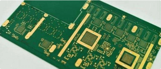
Printed Circuit Board (PCB) manufacturing is a complex, multi-stage process that transforms raw materials into the foundation of modern electronics. As the backbone of virtually all electronic devices, PCBs provide mechanical support and electrical connections between components through conductive pathways etched from copper sheets laminated onto non-conductive substrates.
The global PCB market has experienced consistent growth, valued at approximately $72 billion in 2022 and projected to reach $89 billion by 2027, with a compound annual growth rate (CAGR) of 4.3%. This growth is driven by increasing demand across industries such as consumer electronics, automotive, aerospace, and medical devices.
This article provides a detailed examination of PCB manufacturing processes, materials, technologies, and quality control measures that ensure reliable performance in electronic applications.
PCB Materials and Stack-up
Substrate Materials
The choice of substrate material significantly impacts a PCB’s performance, durability, and cost:
- FR-4: The most common substrate, a glass-reinforced epoxy laminate, offering good mechanical strength and electrical insulation (Dielectric constant ~4.3-4.8 at 1 MHz)
- High-Frequency Laminates: Materials like Rogers RO4000® or PTFE for RF/microwave applications with stable dielectric constants (Dk 2.2-10.2) and low loss tangents (0.0009-0.0025)
- Metal Core PCBs: Aluminum or copper-based boards for high-power applications requiring efficient heat dissipation
- Flexible Substrates: Polyimide films (e.g., Kapton) for flexible circuits with excellent thermal stability (-269°C to +400°C)
Copper Foil
PCB manufacturers typically use electrodeposited (ED) or rolled annealed (RA) copper foil in weights ranging from 0.5 oz/ft² (17.5 µm) to 2 oz/ft² (70 µm). High-frequency applications may employ low-profile foils to reduce skin effect losses.
Layer Stack-up Design
Modern PCBs utilize sophisticated multilayer configurations:
- Signal Layers: For component interconnections
- Power Planes: Distribute stable voltage
- Ground Planes: Provide shielding and return paths
- Dielectric Layers: Separate conductive layers
A typical 4-layer stack-up might arrange layers as:
- Top Signal
- Ground Plane
- Power Plane
- Bottom Signal
PCB Manufacturing Process
Step 1: Design and Preparation
The manufacturing process begins with the PCB design files (Gerber, ODB++, IPC-2581) containing information about:
- Layer stack-up
- Copper traces
- Drill locations
- Solder mask
- Silkscreen
Manufacturers perform Design for Manufacturability (DFM) checks to identify potential issues before production.
Step 2: Inner Layer Processing
For multilayer boards, the inner layers undergo:
- Cleaning: Removal of contaminants
- Lamination: Dry film resist application
- Exposure: UV light transfers the circuit pattern
- Development: Unexposed resist is removed
- Etching: Copper removal (typically using ammonium persulfate or cupric chloride)
- Strip: Removal of remaining resist
- AOI: Automated Optical Inspection verifies pattern accuracy
Step 3: Layer Alignment and Lamination
The inner layers are precisely aligned using registration holes and laminated under heat (typically 170-180°C) and pressure (200-300 psi) with prepreg (pre-impregnated) dielectric material and outer copper foil.
Step 4: Drilling
High-speed CNC drilling machines create:
- Through holes (0.15mm to 6.35mm diameter)
- Blind/buried vias
- Microvias (<0.15mm diameter)
Drilling parameters are critical:
- Spindle speed: 80,000-150,000 RPM
- Feed rate: 1.5-4.0 m/min
- Retract rate: 10-20 m/min
Step 5: Plating and Metallization
The drilled holes are metallized to create electrical connections between layers:
- Desmear: Removes resin residue
- Electroless Copper Deposition: 0.3-0.8 µm thick seed layer
- Electroplating: Builds up copper thickness (typically 25 µm)
- Surface Finishes: Such as:
- HASL (Hot Air Solder Leveling)
- ENIG (Electroless Nickel Immersion Gold)
- OSP (Organic Solderability Preservative)
- Immersion Silver
Step 6: Outer Layer Processing
Similar to inner layers but with additional steps for component mounting:
- Pattern plating
- Tin plating as etch resist
- Etching
- Tin stripping
- Solder mask application (LPI, dry film, or liquid photoimageable)
- Silkscreen printing
- Surface finish application
Step 7: Electrical Testing
Final verification includes:
- Continuity Testing: Ensures all connections exist
- Isolation Testing: Verifies no unintended shorts
- Impedance Testing: For controlled impedance boards
- Flying Probe or Fixture Testing: Depending on volume
Advanced PCB Technologies
High-Density Interconnect (HDI)
HDI PCBs feature:
- Microvias (≤0.15mm diameter)
- Fine pitch traces (<0.1mm width/space)
- Sequential lamination
- Any-layer via structures
HDI technology enables 20-30% size reduction and improved signal integrity.
Embedded Components
Passive components (resistors, capacitors) are embedded within the PCB layers, offering:
- Reduced footprint
- Improved electrical performance
- Enhanced reliability
Flexible and Rigid-Flex PCBs
Combining rigid and flexible sections allows for:
- 3D packaging
- Dynamic flexing
- Reduced interconnection points
Quality Control and Standards
PCB manufacturers adhere to several industry standards:
- IPC-A-600: Acceptability of Printed Boards
- IPC-6012: Qualification and Performance Specification for Rigid PCBs
- IPC-6013: For Flexible PCBs
- IPC-7351: Land Pattern Standards
Key quality metrics include:
- Dimensional Tolerance: Typically ±0.1mm
- Hole Position Accuracy: ±0.05-0.1mm
- Copper Thickness: ±10% of specified
- Solder Mask Thickness: 10-30 µm
Environmental Considerations
Modern PCB manufacturing addresses environmental concerns through:
- Lead-Free Processes: Compliance with RoHS directives
- Waste Reduction: Recycling of copper, water, and chemicals
- Alternative Materials: Halogen-free laminates
- Energy Efficiency: Optimized production processes
Future Trends in PCB Manufacturing
Emerging technologies shaping PCB fabrication include:
- Additive Manufacturing: 3D printed electronics
- Embedded Actives: Integration of semiconductor devices
- Advanced Materials: Nanocomposites, graphene conductors
- AI-Driven Optimization: For design and manufacturing
- Higher Frequency Materials: For 5G and mmWave applications
Conclusion
PCB manufacturing continues to evolve, driven by the relentless demand for smaller, faster, and more reliable electronic devices. The industry’s ability to innovate in materials, processes, and design methodologies ensures that printed circuit boards will remain fundamental to electronic products across all sectors. As technologies like IoT, 5G, and AI advance, PCB manufacturers will face new challenges in meeting the requirements for higher frequencies, increased density, and enhanced reliability—all while maintaining cost-effectiveness and environmental sustainability.
Understanding the complete PCB manufacturing process enables designers and engineers to create more manufacturable, reliable, and cost-effective solutions, ultimately contributing to better electronic products that power our modern world.


