Pcb manufacturing capabilities
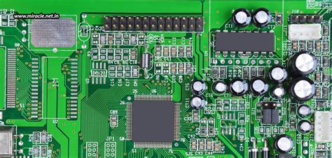
Advanced Surface Mount Technology (SMT) Techniques
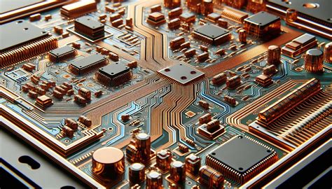
Advanced Surface Mount Technology (SMT) techniques have revolutionized the field of PCB manufacturing, offering unparalleled precision, efficiency, and reliability. As the demand for smaller, more complex electronic devices continues to grow, the capabilities of SMT have expanded to meet these challenges.
One of the key advancements in SMT is the development of high-speed pick-and-place machines.
These machines are capable of placing thousands of components per hour with remarkable accuracy, significantly reducing production time and costs. The integration of vision systems in these machines ensures that components are placed with exact precision, minimizing errors and enhancing the overall quality of the final product.
In addition to high-speed placement, the use of advanced soldering techniques has also contributed to the evolution of SMT.
Reflow soldering, for instance, has become a standard process in PCB manufacturing. This technique involves applying solder paste to the PCB, placing the components, and then heating the assembly in a reflow oven. The controlled heating process ensures that the solder paste melts and forms reliable connections between the components and the PCB. The use of nitrogen in the reflow process further enhances the quality of the solder joints by reducing oxidation and improving wetting properties.
Another significant advancement in SMT is the implementation of automated optical inspection (AOI) systems.
These systems use high-resolution cameras and sophisticated algorithms to inspect PCBs for defects such as misaligned components, solder bridges, and insufficient solder joints. By identifying and addressing these issues early in the production process, AOI systems help to ensure the reliability and performance of the final product. Moreover, the data collected by AOI systems can be used to continuously improve the manufacturing process, leading to higher yields and reduced costs.
The miniaturization of electronic components has also driven the development of advanced SMT techniques.
The use of micro-components, such as 0201 and 01005 packages, requires precise placement and soldering capabilities. To address this challenge, manufacturers have developed specialized equipment and processes that can handle these tiny components with high accuracy. For example, stencil printing technology has evolved to accommodate the fine pitch and small apertures required for micro-components. Laser-cut stencils and advanced printing techniques ensure that solder paste is applied accurately and consistently, which is critical for achieving reliable solder joints.
Furthermore, the adoption of lead-free soldering has become increasingly important in SMT due to environmental regulations and industry standards.
Lead-free soldering presents unique challenges, such as higher melting temperatures and different wetting properties compared to traditional lead-based solders. To address these challenges, manufacturers have developed specialized solder alloys and reflow profiles that ensure reliable solder joints while complying with environmental regulations.
In conclusion, the advancements in Surface Mount Technology have significantly enhanced the capabilities of PCB manufacturing. High-speed pick-and-place machines, advanced soldering techniques, automated optical inspection systems, and the ability to handle micro-components are just a few examples of how SMT has evolved to meet the demands of modern electronics. As technology continues to advance, it is likely that SMT techniques will continue to improve, further pushing the boundaries of what is possible in PCB manufacturing. The ongoing innovation in this field not only ensures the production of high-quality electronic devices but also contributes to the overall progress of the electronics industry.
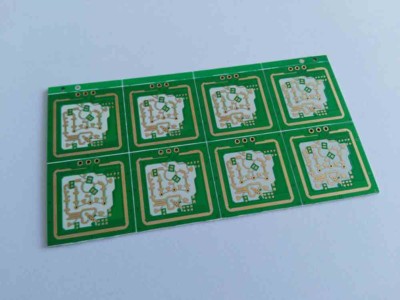
High-Density Interconnect (HDI) PCB Fabrication
High-Density Interconnect (HDI) PCB fabrication represents a significant advancement in the field of printed circuit board manufacturing, offering numerous benefits that cater to the ever-evolving demands of modern electronic devices. As technology continues to progress, the need for more compact, efficient, and high-performing electronic components has become paramount. HDI PCBs address these needs by incorporating advanced design techniques and manufacturing processes that enable the creation of highly intricate and densely packed circuit boards.
One of the primary advantages of HDI PCB fabrication is the ability to achieve higher component density.
This is accomplished through the use of microvias, blind vias, and buried vias, which allow for more interconnections within a smaller area. Microvias, in particular, are essential in HDI designs as they enable the creation of finer lines and spaces, thus facilitating the placement of more components on a single board. This increased density not only enhances the overall performance of the electronic device but also contributes to a reduction in its size and weight, making it ideal for applications in smartphones, tablets, and other portable gadgets.
Moreover, HDI PCBs offer improved signal integrity and electrical performance.
The shorter interconnect paths and reduced parasitic effects associated with HDI designs result in lower signal loss and faster signal transmission. This is particularly beneficial in high-frequency applications where maintaining signal integrity is crucial. Additionally, the use of advanced materials and fabrication techniques in HDI PCBs helps to minimize electromagnetic interference (EMI) and crosstalk, further enhancing the reliability and performance of the final product.
Transitioning to the manufacturing process, HDI PCB fabrication involves several sophisticated steps that require precision and expertise.
The process begins with the design phase, where advanced computer-aided design (CAD) software is used to create detailed layouts that incorporate the necessary microvias and interconnects. Once the design is finalized, the fabrication process commences with the creation of the substrate, typically made from high-quality materials such as FR4 or polyimide. The substrate is then layered with copper and subjected to a series of photolithographic and etching processes to form the intricate circuitry.
Following the formation of the circuitry, the next step involves the drilling of microvias, which is achieved using laser drilling technology.
This method ensures the creation of precise and clean microvias that are essential for the high-density interconnects. Subsequently, the microvias are plated with copper to establish electrical connections between the different layers of the PCB. The board then undergoes additional processes such as lamination, solder mask application, and surface finish to complete the fabrication.
Furthermore, quality control is a critical aspect of HDI PCB fabrication.
Rigorous testing and inspection procedures are implemented at various stages of the manufacturing process to ensure that the final product meets the stringent requirements of modern electronic applications. Techniques such as automated optical inspection (AOI), X-ray inspection, and electrical testing are employed to detect any defects or inconsistencies that may compromise the performance of the PCB.
In conclusion, HDI PCB fabrication is a cutting-edge technology that addresses the growing demands for miniaturization, enhanced performance, and reliability in electronic devices. By leveraging advanced design techniques and manufacturing processes, HDI PCBs offer numerous advantages, including higher component density, improved signal integrity, and superior electrical performance. As the electronics industry continues to evolve, the importance of HDI PCB fabrication will undoubtedly increase, driving further innovations and advancements in the field.
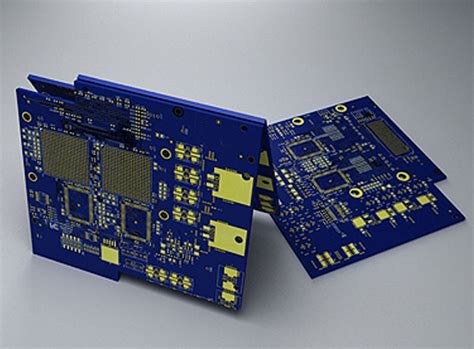
Multilayer PCB Manufacturing Processes
Multilayer PCB manufacturing processes are intricate and require a high degree of precision and expertise. These processes are essential for creating the complex circuit boards that power modern electronic devices. The journey begins with the design phase, where engineers use sophisticated software to create detailed schematics and layouts. This design is then translated into a series of layers, each representing a different part of the circuit. The number of layers can vary, but it is not uncommon to see multilayer PCBs with anywhere from four to over twenty layers.
Once the design is finalized, the manufacturing process commences with the creation of the individual layers.
Each layer starts as a thin sheet of substrate material, typically made of fiberglass-reinforced epoxy resin, known as FR4. This substrate is coated with a layer of copper, which will form the conductive pathways of the circuit. The copper is then etched away using a photolithographic process, leaving behind the desired circuit pattern. This process is repeated for each layer, ensuring that all the necessary pathways are accurately created.
Following the etching process, the individual layers must be aligned and laminated together.
This is a critical step, as any misalignment can result in a malfunctioning PCB. The layers are stacked in the correct order and then subjected to heat and pressure in a lamination press. This causes the layers to bond together, forming a single, solid board. The lamination process also includes the insertion of pre-preg materials, which are sheets of fiberglass impregnated with resin. These materials help to insulate the layers and provide additional structural integrity.
After lamination, the next step is drilling. Precision drilling machines create holes in the PCB, which will later be used to connect the different layers electrically.
These holes, known as vias, are then plated with copper to ensure a reliable electrical connection. The plating process involves immersing the board in a series of chemical baths, which deposit a thin layer of copper onto the walls of the holes.
Once the vias are plated, the outer layers of the PCB are processed.
This involves a similar photolithographic and etching process as the inner layers, creating the final circuit pattern on the surface of the board. Additional plating processes may be used to apply a protective layer of tin or gold to the exposed copper, preventing oxidation and improving solderability.
The final steps in the manufacturing process include solder mask application, silkscreen printing, and electrical testing.
The solder mask is a protective layer that covers the entire surface of the PCB, except for the areas where components will be soldered. This helps to prevent short circuits and other issues during assembly. The silkscreen is used to print labels and other information on the board, aiding in component placement and identification. Electrical testing is performed to ensure that the PCB functions correctly and meets all design specifications.
In conclusion, multilayer PCB manufacturing processes are complex and require a high level of precision and expertise. From the initial design phase to the final testing, each step is critical to producing a reliable and functional circuit board. Advances in technology continue to push the boundaries of what is possible, enabling the creation of ever more sophisticated electronic devices.
Rigid-Flex PCB Production Capabilities
Rigid-flex PCB production capabilities have significantly evolved, offering a blend of the best features from both rigid and flexible circuit boards. This hybrid technology is increasingly becoming the cornerstone of modern electronic design, providing unparalleled versatility and reliability. The production of rigid-flex PCBs involves a meticulous process that combines the durability of rigid boards with the adaptability of flexible circuits, resulting in a product that can meet the demanding requirements of various applications.
One of the primary capabilities in rigid-flex PCB production is the ability to design complex multilayer boards.
These boards can incorporate multiple layers of both rigid and flexible materials, allowing for intricate circuit designs that can fit into compact and irregularly shaped spaces. This is particularly advantageous in industries such as aerospace, medical devices, and consumer electronics, where space constraints and performance reliability are critical. The integration of rigid and flexible layers also reduces the need for connectors and cables, thereby minimizing potential points of failure and enhancing overall system reliability.
Another significant capability is the precision in manufacturing processes.
Advanced fabrication techniques, such as laser drilling and high-resolution imaging, enable the production of fine lines and spaces, which are essential for high-density interconnect (HDI) applications. These techniques ensure that the electrical performance of the rigid-flex PCB is optimized, with minimal signal loss and interference. Additionally, the use of automated optical inspection (AOI) and electrical testing throughout the production process ensures that each board meets stringent quality standards, thereby reducing the risk of defects and improving product reliability.
Material selection is also a critical aspect of rigid-flex PCB production.
The choice of materials, including polyimide for flexible layers and FR4 for rigid sections, plays a crucial role in determining the board’s performance characteristics. Polyimide is favored for its excellent thermal stability and flexibility, while FR4 provides mechanical strength and rigidity. The combination of these materials allows the rigid-flex PCB to withstand harsh environmental conditions, such as extreme temperatures and mechanical stress, making it suitable for a wide range of applications.
Furthermore, the ability to incorporate various surface finishes and protective coatings enhances the durability and longevity of rigid-flex PCBs.
Surface finishes such as ENIG (Electroless Nickel Immersion Gold) and HASL (Hot Air Solder Leveling) provide excellent solderability and corrosion resistance, ensuring reliable electrical connections. Protective coatings, such as conformal coatings and solder masks, offer additional protection against moisture, dust, and chemical contaminants, thereby extending the lifespan of the PCB.
The design flexibility offered by rigid-flex PCBs is another notable capability.
Engineers can create designs that fold, twist, and bend to fit into compact spaces without compromising the integrity of the electrical connections. This flexibility is particularly beneficial in applications where dynamic movement is required, such as wearable devices and robotics. The ability to design three-dimensional circuits also opens up new possibilities for innovative product designs, enabling the development of more compact and lightweight electronic devices.
In conclusion, the production capabilities of rigid-flex PCBs have advanced to meet the growing demands of modern electronic applications. The combination of complex multilayer designs, precision manufacturing processes, careful material selection, and enhanced durability features makes rigid-flex PCBs a versatile and reliable solution for a wide range of industries. As technology continues to evolve, the capabilities of rigid-flex PCB production are expected to expand further, driving innovation and enabling the development of next-generation electronic devices.
Quality Control in PCB Manufacturing
Quality control in PCB manufacturing is a critical aspect that ensures the reliability and performance of the final product. The process begins with the selection of high-quality raw materials, which is fundamental to achieving a robust and durable printed circuit board. Manufacturers meticulously choose substrates, copper foils, and other essential components, adhering to stringent industry standards. This initial step sets the foundation for the entire manufacturing process, as the quality of materials directly impacts the board’s functionality and longevity.
Following material selection, the design phase incorporates various quality control measures.
Advanced software tools are employed to simulate and verify the design, ensuring that it meets all specified requirements. Design for manufacturability (DFM) checks are conducted to identify potential issues that could arise during production. These checks help in minimizing errors and optimizing the design for efficient manufacturing. By addressing potential problems early in the design phase, manufacturers can prevent costly rework and delays later in the process.
As the manufacturing process progresses, each stage is subject to rigorous inspection and testing.
During the fabrication of the PCB, automated optical inspection (AOI) systems are utilized to detect defects such as misalignments, shorts, and opens. These systems use high-resolution cameras and sophisticated algorithms to compare the fabricated board against the original design files. Any discrepancies are flagged for further examination, ensuring that only defect-free boards move forward in the production line.
In addition to AOI, electrical testing is a crucial component of quality control.
This involves subjecting the PCB to various electrical tests to verify its functionality and performance. Flying probe testers and in-circuit testers (ICT) are commonly used to check for continuity, isolation, and proper component placement. These tests help in identifying any electrical faults that could compromise the board’s operation. By thoroughly testing each board, manufacturers can guarantee that the final product meets the required specifications and performs reliably in its intended application.
Environmental testing is another essential aspect of quality control in PCB manufacturing.
PCBs are often exposed to harsh conditions, such as extreme temperatures, humidity, and mechanical stress. To ensure that the boards can withstand these conditions, manufacturers conduct a series of environmental tests, including thermal cycling, humidity resistance, and vibration testing. These tests simulate real-world conditions and help in identifying any potential weaknesses in the board’s design or construction. By subjecting the PCBs to rigorous environmental testing, manufacturers can ensure that the final product is robust and reliable.
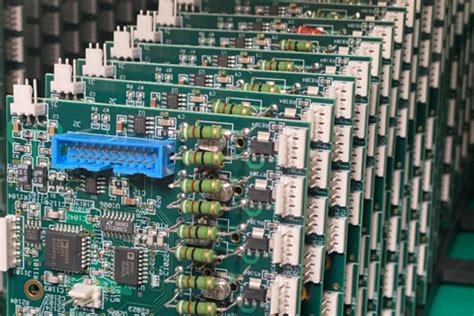
Furthermore, quality control extends to the assembly process, where components are mounted onto the PCB.
Surface mount technology (SMT) and through-hole technology (THT) are commonly used for component placement. During this stage, automated placement machines and soldering equipment are calibrated to precise specifications to ensure accurate and reliable assembly. Post-assembly inspections, including X-ray inspection and functional testing, are conducted to verify the integrity of the solder joints and the overall functionality of the assembled board.
In conclusion, quality control in PCB manufacturing is a comprehensive process that encompasses every stage of production, from material selection to final assembly. By implementing stringent quality control measures, manufacturers can ensure that their PCBs meet the highest standards of reliability and performance. This meticulous approach not only enhances the quality of the final product but also instills confidence in customers, knowing that they are receiving a product that has been thoroughly tested and verified.