PCB Manufacturing Capabilities: A Comprehensive Overview
Introduction
Printed Circuit Boards (PCBs) are the backbone of modern electronics, serving as the foundation for nearly all electronic devices, from smartphones and computers to industrial machinery and medical equipment. As technology advances, the demand for high-quality, reliable, and complex PCBs continues to grow. PCB manufacturers must continuously enhance their capabilities to meet these evolving requirements.
This article explores the key aspects of PCB manufacturing capabilities, including materials, layer counts, precision, advanced technologies, and quality control measures. Understanding these capabilities helps engineers and designers select the right manufacturer for their specific needs.
1. PCB Materials and Substrates
The choice of materials significantly impacts PCB performance, durability, and application suitability. Manufacturers must offer a variety of substrate options to meet different design requirements.
Common PCB Materials:
- FR-4: The most widely used material, made from fiberglass and epoxy resin. It provides good mechanical strength, electrical insulation, and flame resistance.
- High-Frequency Laminates: Used in RF and microwave applications (e.g., Rogers, PTFE). These materials minimize signal loss at high frequencies.
- Metal Core PCBs (MCPCBs): Utilize aluminum or copper cores for superior heat dissipation, ideal for LED lighting and power electronics.
- Flexible and Rigid-Flex PCBs: Made from polyimide or similar flexible materials, enabling bendable circuits for wearables, medical devices, and aerospace applications.
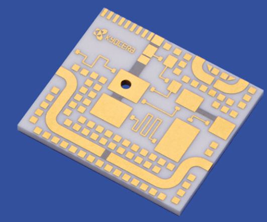
- Ceramic-Based PCBs: Used in high-temperature and high-power applications due to their excellent thermal conductivity.
2. Layer Count and Stackup Configurations
PCBs can range from single-layer to high-density multilayer boards (up to 50+ layers). The layer count depends on circuit complexity, signal integrity requirements, and space constraints.
- Single/Double-Layer PCBs: Simple designs for low-cost consumer electronics.
- Multilayer PCBs (4-12 layers): Common in computing, telecommunications, and automotive electronics.
- High-Density Interconnect (HDI) PCBs: Feature microvias, blind/buried vias, and fine traces for compact, high-performance devices like smartphones.
- Advanced Stackups: Manufacturers must support impedance-controlled designs, mixed-signal layouts, and embedded passive components.
3. Precision and Manufacturing Tolerances
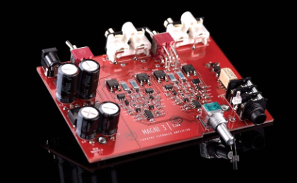
As electronic devices shrink, PCB manufacturers must achieve tighter tolerances in trace width, spacing, and hole sizes.
Key Precision Metrics:
- Minimum Trace/Space: Advanced manufacturers achieve 3/3 mil (0.075 mm) or finer for HDI designs.
- Drilling Tolerance: Laser drills can create microvias as small as 0.1 mm, while mechanical drills handle larger through-holes.
- Registration Accuracy: Critical for multilayer alignment, with high-end manufacturers maintaining ±25 µm or better.
- Surface Finish Options:
- HASL (Hot Air Solder Leveling) – Traditional, cost-effective.
- ENIG (Electroless Nickel Immersion Gold) – Excellent for fine-pitch components.
- OSP (Organic Solderability Preservative) – Environmentally friendly but less durable.
- Immersion Silver/Tin – Alternative to ENIG for specific applications.
4. Advanced PCB Technologies
To stay competitive, manufacturers must support cutting-edge PCB technologies:
High-Density Interconnect (HDI)
- Uses laser-drilled microvias, stacked vias, and ultra-fine traces to increase routing density.
- Essential for smartphones, IoT devices, and miniaturized electronics.
Embedded Components
- Passive components (resistors, capacitors) are embedded within the PCB layers, saving space and improving signal integrity.
Rigid-Flex and Flexible PCBs
- Combine rigid and flexible sections, reducing connectors and improving reliability in dynamic applications (e.g., foldable phones, medical implants).
High-Speed and RF PCBs
- Require controlled impedance, low-loss materials, and precise signal integrity analysis.
- Used in 5G networks, radar systems, and high-frequency communication devices.
Thermal Management Solutions
- Heavy copper PCBs (up to 20 oz) for high-current applications.
- Metal-core and thermally conductive dielectric materials for heat dissipation.
5. PCB Fabrication Processes
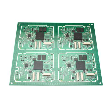
A robust PCB manufacturing process involves multiple stages, each requiring precision and quality control:
- Design & DFM Check – Engineers review Gerber files for manufacturability.
- Material Selection – Choosing the right substrate and copper weight.
- Imaging & Etching – UV exposure and chemical etching define circuit patterns.
- Lamination & Layer Alignment – Multilayer PCBs require precise layer stacking.
- Drilling & Plating – Mechanical or laser drilling followed by copper plating.
- Solder Mask & Silkscreen – Applying protective coatings and component labels.
- Surface Finish Application – ENIG, HASL, or other finishes for solderability.
- Electrical Testing & Inspection – Automated Optical Inspection (AOI), flying probe testing, and impedance verification.
6. Quality Control and Certifications
Reliable PCB manufacturers adhere to strict quality standards, including:
- IPC-A-600 – Acceptability of Printed Boards.
- IPC-6012 – Qualification and Performance Specifications.
- ISO 9001 – Quality Management Systems.
- UL Certification – Safety compliance for specific applications.
- RoHS & REACH Compliance – Ensuring lead-free and environmentally friendly production.
Advanced testing methods include:
- Automated Optical Inspection (AOI) – Detects defects in traces and solder masks.
- X-Ray Inspection – Checks internal layer alignment and via integrity.
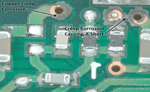
- Electrical Testing – Continuity and isolation tests to ensure functionality.
7. Turnaround Time and Scalability
Manufacturers must balance speed and quality:
- Prototype PCBs – Fast-turn services (24-72 hours) for design validation.
- Mass Production – Scalable processes with lead times ranging from days to weeks, depending on complexity.
- Supply Chain Management – Reliable sourcing of raw materials to avoid delays.
Conclusion
PCB manufacturing capabilities have expanded dramatically to meet the demands of modern electronics. From advanced HDI and rigid-flex designs to high-speed and thermal management solutions, manufacturers must continuously innovate to stay competitive. Engineers must carefully evaluate a manufacturer’s material options, precision tolerances, technological expertise, and quality certifications to ensure optimal PCB performance.
As the industry evolves, trends like 3D-printed electronics, AI-driven design optimization, and sustainable manufacturing will further shape PCB production. Choosing the right manufacturing partner with cutting-edge capabilities is crucial for success in today’s fast-paced electronics market.

