Pcb manufacturing etching
Innovations In PCB Etching Techniques
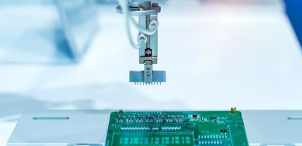
In the realm of printed circuit board (PCB) manufacturing, etching stands as a pivotal process that defines the precision and functionality of the final product. As technology advances, innovations in PCB etching techniques have become essential to meet the growing demands for smaller, more efficient, and highly reliable electronic devices. These innovations not only enhance the quality of PCBs but also contribute to more sustainable manufacturing practices.
Traditionally, PCB etching involved the use of chemical solutions to remove unwanted copper from the board, leaving behind the desired circuit pattern.
However, this method often posed challenges such as environmental concerns due to the disposal of hazardous chemicals and limitations in achieving finer circuit patterns. In response to these challenges, the industry has witnessed significant advancements in etching techniques, which have revolutionized the manufacturing process.
One of the most notable innovations is the advent of laser etching technology.
Unlike chemical etching, laser etching employs high-precision lasers to ablate unwanted copper from the PCB surface. This method offers several advantages, including the ability to achieve extremely fine circuit patterns with high accuracy. Moreover, laser etching is a non-contact process, which reduces the risk of physical damage to the board. This technique also minimizes waste generation, aligning with the industry’s shift towards more environmentally friendly practices.
In addition to laser etching, the development of plasma etching has also garnered attention.
Plasma etching utilizes ionized gases to remove material from the PCB surface. This technique is particularly effective for etching complex multilayer boards, as it provides excellent control over the etching depth and uniformity. Plasma etching is also advantageous in terms of its ability to handle a wide range of materials, making it a versatile option for manufacturers looking to produce diverse PCB designs.
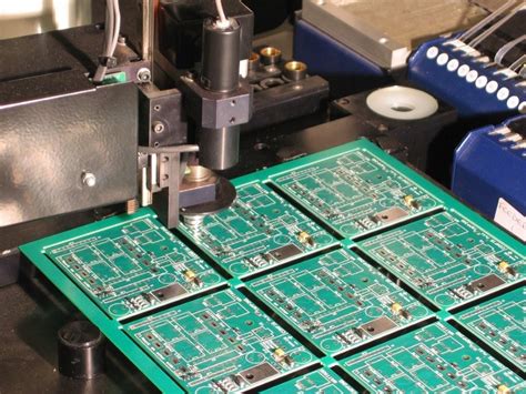
Furthermore, the integration of automation and artificial intelligence (AI) in PCB etching processes has led to significant improvements in efficiency and precision.
Automated systems equipped with AI algorithms can optimize etching parameters in real-time, ensuring consistent quality across large production volumes. This not only reduces the likelihood of defects but also enhances the overall throughput of the manufacturing process. As a result, manufacturers can meet the increasing demand for high-performance PCBs in a cost-effective manner.
Another promising innovation is the use of environmentally benign etching solutions.
Researchers have been exploring alternative etching chemicals that are less harmful to the environment while maintaining the efficacy of traditional methods. These green etching solutions aim to reduce the ecological footprint of PCB manufacturing, addressing the growing concerns over sustainability in the electronics industry.
In conclusion, the innovations in PCB etching techniques have significantly transformed the landscape of circuit board manufacturing. From laser and plasma etching to the integration of automation and the development of eco-friendly solutions, these advancements have paved the way for more precise, efficient, and sustainable production processes. As the demand for sophisticated electronic devices continues to rise, the ongoing evolution of etching techniques will undoubtedly play a crucial role in shaping the future of PCB manufacturing. By embracing these innovations, manufacturers can not only enhance the quality and performance of their products but also contribute to a more sustainable and technologically advanced world.
Environmental Impact Of PCB Etching Processes
The process of etching in printed circuit board (PCB) manufacturing is a critical step that involves the removal of unwanted copper from a laminated board to create the desired circuit patterns. While this process is essential for the production of electronic devices, it also poses significant environmental challenges. Understanding the environmental impact of PCB etching processes is crucial for developing more sustainable manufacturing practices.
To begin with, the etching process typically involves the use of chemical solutions, such as ferric chloride, ammonium persulfate,
or cupric chloride, which are effective in dissolving excess copper. However, these chemicals can be hazardous if not managed properly. The disposal of spent etching solutions is a major environmental concern, as they contain high concentrations of copper ions and other potentially harmful substances. If these solutions are released into the environment without adequate treatment, they can contaminate water sources, harm aquatic life, and disrupt ecosystems.
Moreover, the etching process generates a significant amount of waste, including copper sludge and other by-products.
The management of this waste is another critical environmental issue. Improper disposal can lead to soil contamination and pose risks to human health. Therefore, it is imperative for PCB manufacturers to implement effective waste management strategies, such as recycling and recovery of copper from sludge, to minimize environmental impact.
In addition to chemical waste, the etching process also consumes a considerable amount of water and energy.
The use of large volumes of water for rinsing and cleaning can strain local water resources, especially in regions where water scarcity is a concern. Furthermore, the energy-intensive nature of the etching process contributes to the carbon footprint of PCB manufacturing. As the demand for electronic devices continues to grow, so does the need for more sustainable practices that reduce water and energy consumption.
Transitioning to more environmentally friendly etching methods is a promising solution to these challenges.
For instance, some manufacturers are exploring the use of alternative etching techniques, such as laser etching, which eliminates the need for chemical solutions and reduces waste generation. Additionally, advancements in closed-loop systems allow for the recycling and reuse of etching solutions, thereby minimizing the release of hazardous substances into the environment.
Furthermore, regulatory frameworks play a crucial role in mitigating the environmental impact of PCB etching processes.
Governments and environmental agencies are increasingly imposing stricter regulations on the disposal of chemical waste and emissions from manufacturing facilities. Compliance with these regulations not only helps protect the environment but also encourages manufacturers to adopt cleaner technologies and practices.
In conclusion, while PCB etching is an indispensable part of electronic manufacturing, it presents several environmental challenges that need to be addressed. By adopting sustainable practices, such as alternative etching methods, effective waste management, and compliance with environmental regulations, the industry can significantly reduce its ecological footprint. As technology continues to evolve, it is essential for manufacturers to prioritize environmental considerations in their operations, ensuring that the growth of the electronics industry does not come at the expense of the planet’s health. Through concerted efforts and innovation, it is possible to achieve a balance between technological advancement and environmental sustainability.
Comparing Wet And Dry Etching Methods In PCB Manufacturing
In the realm of printed circuit board (PCB) manufacturing, etching is a critical process that defines the intricate pathways for electrical connectivity. This process involves the removal of unwanted copper from a laminated board to create the desired circuit patterns. Two primary methods of etching are employed in the industry: wet etching and dry etching. Each method has its own set of advantages and limitations, making the choice between them dependent on specific manufacturing requirements and constraints.
Wet etching is the more traditional of the two methods and involves the use of chemical solutions to dissolve unwanted copper.
Typically, an acid or alkaline solution is applied to the PCB, which selectively removes the exposed copper areas. One of the main advantages of wet etching is its cost-effectiveness, as the chemicals used are generally inexpensive and the process can be easily scaled for large production runs. Additionally, wet etching is known for its simplicity and ease of implementation, making it a popular choice for many manufacturers. However, it is not without its drawbacks. The process can be less precise than dry etching, as the chemical solutions can undercut the resist, leading to less defined circuit patterns. Furthermore, the disposal of chemical waste poses environmental concerns, necessitating stringent waste management protocols.
In contrast, dry etching employs physical or chemical means to remove material, often using plasma or ion beams.
This method offers greater precision and control, allowing for the creation of finer and more intricate circuit patterns. Dry etching is particularly advantageous for applications requiring high-density interconnects or when working with advanced materials that are not amenable to wet etching. The precision of dry etching also reduces the risk of undercutting, resulting in more accurate and reliable circuit paths. However, these benefits come at a higher cost. The equipment required for dry etching is more complex and expensive, and the process itself can be slower than wet etching. Additionally, the operational expertise required to manage dry etching systems can be a barrier for some manufacturers.
When comparing these two methods, it is essential to consider the specific requirements of the PCB being manufactured.
For high-volume production where cost is a significant factor, wet etching may be the preferred choice. Its ability to efficiently process large batches of PCBs makes it ideal for consumer electronics and other applications where precision is not the primary concern. On the other hand, for applications demanding high precision and complexity, such as aerospace or medical devices, dry etching may be more suitable despite its higher cost. The choice between wet and dry etching is not merely a matter of cost versus precision; it also involves considerations of environmental impact, production speed, and material compatibility.
In conclusion, both wet and dry etching methods have their place in PCB manufacturing, each offering distinct advantages that cater to different needs. As technology advances and the demand for more sophisticated electronic devices grows, manufacturers must carefully evaluate these methods to determine the most appropriate approach for their specific applications. By understanding the nuances of each etching technique, manufacturers can optimize their processes, balancing cost, precision, and environmental responsibility to achieve the best possible outcomes in PCB production.
Safety Measures In PCB Etching Operations
In the realm of printed circuit board (PCB) manufacturing, etching is a critical process that involves the removal of unwanted copper from a board to create the desired circuit patterns. This process, while essential, involves the use of various chemicals and equipment that can pose significant safety risks if not handled properly. Therefore, implementing stringent safety measures is paramount to ensure the well-being of workers and the integrity of the manufacturing process.
To begin with, understanding the chemicals involved in PCB etching is crucial.
Common etching solutions include ferric chloride, ammonium persulfate, and cupric chloride, each of which can be hazardous if mishandled. These chemicals can cause skin irritation, respiratory issues, and even more severe health problems upon prolonged exposure. Consequently, it is imperative for workers to wear appropriate personal protective equipment (PPE) such as gloves, goggles, and aprons. This protective gear acts as a barrier, minimizing direct contact with harmful substances and reducing the risk of chemical burns or inhalation of toxic fumes.
Moreover, proper ventilation is a key component in maintaining a safe etching environment.
The fumes generated during the etching process can accumulate quickly, leading to poor air quality and potential respiratory hazards. Installing efficient fume extraction systems can significantly mitigate these risks by ensuring that harmful vapors are promptly removed from the workspace. Additionally, regular maintenance of these systems is essential to ensure their optimal performance and to prevent any unexpected failures that could compromise worker safety.
In addition to PPE and ventilation, training and education play a vital role in promoting safety in PCB etching operations. Workers should be thoroughly trained in the handling and disposal of etching chemicals, as well as in emergency response procedures. This training should be comprehensive and ongoing, with regular updates to reflect any changes in safety protocols or the introduction of new materials and technologies. By fostering a culture of safety awareness, companies can empower their employees to recognize potential hazards and take proactive measures to address them.
Furthermore, the implementation of safety protocols and standard operating procedures (SOPs) is essential in ensuring consistency and safety in etching operations.
These protocols should outline the correct methods for handling chemicals, operating equipment, and responding to emergencies. Regular audits and inspections can help identify any deviations from established procedures, allowing for timely corrective actions to be taken. By adhering to these protocols, companies can minimize the likelihood of accidents and ensure a safe working environment.
Finally, waste management is another critical aspect of safety in PCB etching operations.
The disposal of used etching solutions and other chemical waste must be conducted in accordance with environmental regulations to prevent contamination and harm to the surrounding ecosystem. Implementing proper waste disposal procedures, such as neutralizing chemical residues and using designated disposal facilities, can help mitigate environmental impact and ensure compliance with legal requirements.
In conclusion, safety measures in PCB etching operations are multifaceted, encompassing the use of PPE, effective ventilation, comprehensive training, adherence to SOPs, and responsible waste management. By prioritizing these safety measures, companies can protect their workers, maintain operational efficiency, and uphold their commitment to environmental stewardship. As the PCB manufacturing industry continues to evolve, the importance of safety in etching operations remains a constant, underscoring the need for ongoing vigilance and improvement in safety practices.