Pcb manufacturing impedance control
Understanding The Basics Of Impedance Control In PCB Manufacturing
Impedance control in PCB manufacturing is a critical aspect that ensures the reliable performance of high-speed electronic circuits. As electronic devices become more sophisticated and operate at higher frequencies, the need for precise impedance control becomes increasingly important.
Understanding the basics of impedance control in PCB manufacturing involves delving into the principles of electrical impedance, the factors that influence it, and the methods used to achieve the desired impedance levels.
Electrical impedance is a measure of the opposition that a circuit presents to the flow of alternating current (AC).
It is a complex quantity, consisting of both resistance and reactance, and is influenced by the frequency of the signal. In the context of PCB manufacturing, impedance control refers to the process of designing and fabricating circuit boards with specific impedance characteristics to ensure signal integrity and minimize signal loss. This is particularly crucial for high-speed digital and RF (radio frequency) circuits, where even small deviations in impedance can lead to significant performance issues.
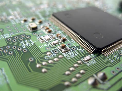
Several factors influence the impedance of a PCB trace, including the trace width, trace thickness, dielectric constant of the substrate material, and the distance between the trace and the reference plane.
The trace width and thickness determine the resistance component of the impedance, while the dielectric constant and the distance to the reference plane affect the capacitive and inductive components. By carefully controlling these parameters during the design and manufacturing process, engineers can achieve the desired impedance levels.
One of the primary methods used to control impedance in PCB manufacturing is the use of controlled impedance traces.
These traces are designed with specific dimensions and are typically placed over a continuous reference plane, such as a ground or power plane. The reference plane helps to maintain a consistent impedance by providing a return path for the signal and minimizing the effects of external interference. Additionally, the use of differential pairs, where two traces are routed in parallel with a specific spacing, can help to achieve controlled impedance and reduce noise.
Another important aspect of impedance control is the selection of the appropriate substrate material.
The dielectric constant of the substrate material plays a significant role in determining the impedance of the traces. Materials with a low dielectric constant, such as PTFE (polytetrafluoroethylene) or certain types of ceramics, are often used for high-frequency applications because they help to minimize signal loss and maintain consistent impedance. Conversely, materials with a higher dielectric constant may be used for lower-frequency applications where impedance control is less critical.
Manufacturing processes also play a crucial role in achieving impedance control.
Precision etching techniques are used to ensure that the trace dimensions are within the specified tolerances. Additionally, advanced inspection and testing methods, such as time-domain reflectometry (TDR) and vector network analysis (VNA), are employed to verify the impedance characteristics of the finished PCB. These methods allow manufacturers to detect and correct any deviations from the desired impedance levels, ensuring that the final product meets the required specifications.
In conclusion, understanding the basics of impedance control in PCB manufacturing is essential for designing and producing high-performance electronic circuits. By carefully considering factors such as trace dimensions, substrate materials, and manufacturing processes, engineers can achieve precise impedance control and ensure the reliable operation of high-speed and RF circuits. As technology continues to advance, the importance of impedance control in PCB manufacturing will only continue to grow, making it a critical area of focus for engineers and manufacturers alike.
Techniques For Achieving Precise Impedance Control In PCB Design
Achieving precise impedance control in PCB design is a critical aspect of modern electronics manufacturing, particularly as devices become more complex and operate at higher frequencies. Impedance control ensures that signals travel through the PCB with minimal distortion, which is essential for maintaining signal integrity and overall device performance. Several techniques can be employed to achieve this level of precision, each contributing to the meticulous balance required in high-frequency PCB design.
One fundamental technique involves the careful selection of materials.
The dielectric constant (Dk) of the substrate material significantly impacts impedance. Materials with a consistent Dk are preferred, as variations can lead to impedance mismatches. Commonly used materials include FR4, Rogers, and Teflon, each offering different properties that can be matched to the specific requirements of the design. By choosing the appropriate material, designers can establish a solid foundation for achieving precise impedance control.
In addition to material selection, the geometry of the PCB traces plays a crucial role.
The width and thickness of the traces, as well as the spacing between them, directly affect the impedance. Microstrip and stripline configurations are commonly used to control impedance. A microstrip involves a trace on the outer layer of the PCB with a reference plane beneath it, while a stripline places the trace between two reference planes. Both configurations allow for precise control of the trace dimensions and spacing, which in turn helps maintain the desired impedance.
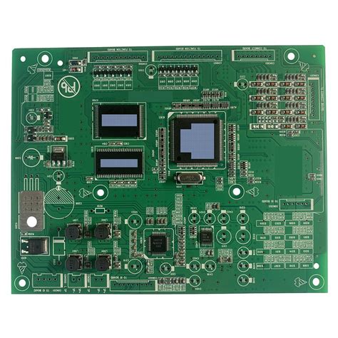
Layer stack-up is another critical factor in impedance control.
The arrangement of the various layers within the PCB, including signal layers and reference planes, must be carefully planned. A well-designed stack-up ensures that the impedance is consistent across different layers and minimizes the risk of signal interference. By strategically placing ground and power planes, designers can create a controlled environment that supports stable impedance throughout the PCB.
Furthermore, the use of simulation tools is indispensable in modern PCB design.
Advanced software allows designers to model and predict the impedance of their designs before physical production. These tools can simulate the effects of different materials, trace geometries, and layer stack-ups, providing valuable insights that guide the design process. By identifying potential issues early, designers can make necessary adjustments to ensure that the final product meets the required impedance specifications.
Manufacturing tolerances also play a significant role in achieving precise impedance control.
Variations in the etching process, for example, can alter the width and spacing of traces, leading to impedance deviations. To mitigate these risks, manufacturers must adhere to stringent quality control measures. This includes using high-precision equipment and regularly calibrating machinery to maintain consistent production standards. By minimizing manufacturing variations, the final PCB is more likely to meet the desired impedance criteria.
Lastly, testing and validation are essential steps in the process.
Once the PCB is manufactured, it must be thoroughly tested to verify that the impedance meets the design specifications. Techniques such as Time Domain Reflectometry (TDR) and Vector Network Analysis (VNA) are commonly used to measure impedance and identify any discrepancies. By conducting rigorous testing, manufacturers can ensure that the PCB performs as intended in real-world applications.
In conclusion, achieving precise impedance control in PCB design requires a multifaceted approach that encompasses material selection, trace geometry, layer stack-up, simulation, manufacturing tolerances, and thorough testing. Each of these elements must be carefully considered and meticulously executed to ensure that the final product meets the stringent requirements of modern electronic devices. Through a combination of advanced techniques and rigorous quality control, designers and manufacturers can achieve the high level of precision necessary for optimal PCB performance.
Common Challenges And Solutions In PCB Impedance Control
Impedance control in PCB manufacturing is a critical aspect that ensures the proper functioning of high-speed electronic circuits. As electronic devices become more sophisticated, the demand for precise impedance control has increased, presenting several challenges that manufacturers must address to maintain signal integrity and overall device performance.
One of the primary challenges in PCB impedance control is the variability in material properties.
The dielectric constant (Dk) and dissipation factor (Df) of the substrate materials can vary significantly between different batches, leading to inconsistencies in impedance. To mitigate this issue, manufacturers often work closely with material suppliers to ensure that the materials used have tightly controlled properties. Additionally, they may implement rigorous incoming inspection processes to verify the material properties before production.
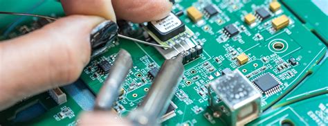
Another significant challenge is the precision required in the PCB fabrication process.
The width and spacing of the traces, the thickness of the copper, and the overall layer stack-up must be meticulously controlled to achieve the desired impedance. Variations in these parameters can lead to deviations from the target impedance, affecting the performance of the circuit. Advanced fabrication techniques, such as laser direct imaging (LDI) and automated optical inspection (AOI), are employed to enhance the precision and consistency of the manufacturing process. These technologies enable manufacturers to produce PCBs with tighter tolerances, thereby improving impedance control.
The design phase also plays a crucial role in impedance control.
Designers must carefully consider the layout of the traces, the placement of components, and the routing of signals to minimize impedance variations. Simulation tools are often used to model the impedance of the PCB and identify potential issues before fabrication. By optimizing the design, manufacturers can reduce the likelihood of impedance-related problems in the final product. Furthermore, collaboration between designers and manufacturers is essential to ensure that the design can be accurately translated into a physical PCB with the desired impedance characteristics.
Environmental factors, such as temperature and humidity, can also impact impedance control.
Changes in temperature can cause the dielectric constant of the substrate material to fluctuate, leading to variations in impedance. To address this, manufacturers may use materials with low thermal coefficients of dielectric constant (TCDk) to minimize the impact of temperature changes. Additionally, environmental control measures, such as maintaining a stable temperature and humidity in the manufacturing facility, can help reduce the variability in impedance.
Testing and validation are critical components of the impedance control process.
Manufacturers use various testing methods, such as time-domain reflectometry (TDR) and vector network analyzers (VNA), to measure the impedance of the PCB and ensure it meets the specified requirements. These tests provide valuable feedback that can be used to fine-tune the manufacturing process and improve impedance control. In some cases, manufacturers may also perform statistical process control (SPC) to monitor and analyze the impedance data, identifying trends and potential issues that need to be addressed.
In conclusion, achieving precise impedance control in PCB manufacturing involves addressing several challenges, including material variability, fabrication precision, design considerations, environmental factors, and rigorous testing. By implementing advanced technologies, optimizing design processes, and maintaining close collaboration between designers and manufacturers, it is possible to overcome these challenges and produce high-quality PCBs with consistent impedance characteristics. This ensures the reliable performance of high-speed electronic circuits, meeting the ever-increasing demands of modern electronic devices.
The Role Of Materials In Impedance Control For High-Frequency PCBs
In the realm of high-frequency printed circuit boards (PCBs), impedance control is a critical factor that significantly influences the performance and reliability of electronic devices. The role of materials in achieving precise impedance control cannot be overstated, as the choice of substrate and conductive materials directly impacts the electrical characteristics of the PCB. Understanding the interplay between these materials and their properties is essential for engineers and designers aiming to optimize high-frequency circuits.
To begin with, the dielectric material used in the PCB substrate plays a pivotal role in impedance control.
The dielectric constant (Dk) and dissipation factor (Df) of the substrate material are key parameters that determine the signal integrity and propagation speed. Materials with a low dielectric constant are preferred for high-frequency applications because they reduce signal delay and minimize losses. For instance, polytetrafluoroethylene (PTFE) and ceramic-filled laminates are commonly used in high-frequency PCBs due to their low Dk values and excellent electrical performance. These materials ensure that the impedance remains consistent across the signal path, thereby enhancing the overall performance of the circuit.
Moreover, the thickness of the dielectric layer is another crucial factor that influences impedance.
A precise control over the dielectric thickness is necessary to maintain the desired impedance levels. Variations in thickness can lead to impedance mismatches, resulting in signal reflections and potential data loss. Advanced manufacturing techniques, such as laser drilling and controlled-depth routing, are employed to achieve the required precision in dielectric thickness. These techniques enable the production of high-frequency PCBs with consistent impedance characteristics, ensuring reliable signal transmission.
In addition to the dielectric material, the choice of conductive materials also affects impedance control.
Copper is the most commonly used conductive material in PCBs due to its excellent electrical conductivity and ease of fabrication. However, the surface roughness of copper can impact the impedance of high-frequency signals. A smoother copper surface reduces signal attenuation and improves impedance control. Techniques such as electroless nickel immersion gold (ENIG) and other surface treatments are used to achieve a smoother copper finish, thereby enhancing the performance of high-frequency PCBs.
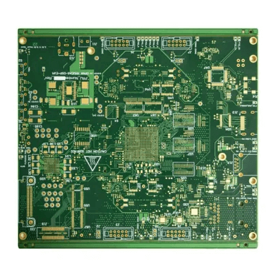
Furthermore, the layout and design of the PCB traces are integral to impedance control.
The width and spacing of the traces, as well as the distance between the signal layers and the ground plane, must be carefully designed to achieve the desired impedance. High-frequency PCBs often employ microstrip or stripline configurations to maintain consistent impedance levels. These configurations involve precise control over the trace dimensions and the dielectric spacing, ensuring that the impedance remains within the specified tolerance.
Transitioning to the manufacturing process, it is essential to consider the impact of material selection on the overall production cost and complexity.
High-frequency PCBs often require specialized materials and advanced fabrication techniques, which can increase the manufacturing cost. However, the benefits of improved signal integrity and performance often outweigh the additional costs. Manufacturers must strike a balance between material properties, design requirements, and cost considerations to achieve optimal impedance control.
In conclusion, the role of materials in impedance control for high-frequency PCBs is multifaceted and involves a careful selection of dielectric and conductive materials, precise control over dielectric thickness, and meticulous design of PCB traces. By understanding and optimizing these factors, engineers and designers can ensure that high-frequency PCBs deliver reliable and high-performance signal transmission, meeting the stringent demands of modern electronic applications.