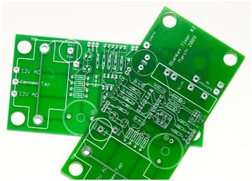
PCB Manufacturing: Key Considerations and Best Practices
Printed Circuit Boards (PCBs) are the backbone of modern electronics, serving as the foundation for nearly all electronic devices. The PCB manufacturing process involves multiple stages, each requiring precision and attention to detail to ensure reliability, performance, and longevity. This article explores the key considerations in PCB manufacturing, covering design, material selection, fabrication, assembly, and testing.
1. PCB Design Considerations
1.1 Schematic and Layout Design
A well-designed schematic is the first step toward a successful PCB. Key considerations include:
- Component Placement: Group related components to minimize trace lengths and reduce noise.
- Trace Width and Spacing: Ensure proper trace width for current-carrying capacity and sufficient spacing to prevent short circuits.
- Signal Integrity: High-speed signals require controlled impedance routing to avoid signal degradation.
- Ground Planes: Proper grounding reduces electromagnetic interference (EMI) and improves stability.
1.2 Design for Manufacturability (DFM)
DFM ensures that the PCB can be efficiently and cost-effectively produced. Key aspects include:
- Minimum Trace/Space Requirements: Follow the manufacturer’s guidelines to avoid fabrication issues.
- Drill Hole Sizes: Ensure holes are large enough for component leads but not excessively large to weaken the board.
- Solder Mask and Silkscreen: Clear markings prevent assembly errors.
2. Material Selection
2.1 Substrate Materials
The choice of PCB substrate affects performance, durability, and cost:
- FR-4: The most common material, suitable for general-purpose applications.
- High-Frequency Materials (Rogers, Teflon): Used in RF and microwave circuits for low signal loss.
- Flexible PCBs (Polyimide): Ideal for wearable and space-constrained devices.
2.2 Copper Thickness
- Standard PCBs use 1 oz/ft² copper, but high-current applications may require 2 oz/ft² or thicker copper layers.
2.3 Surface Finishes
Different finishes impact solderability and durability:
- HASL (Hot Air Solder Leveling): Cost-effective but not ideal for fine-pitch components.
- ENIG (Electroless Nickel Immersion Gold): Provides a flat surface, good for BGA and small components.
- OSP (Organic Solderability Preservative): Eco-friendly but has a limited shelf life.
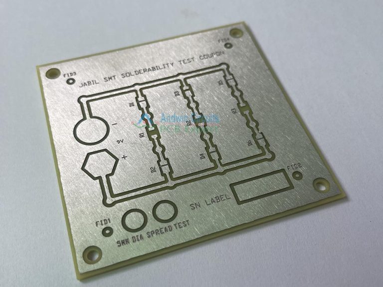
3. PCB Fabrication Process
3.1 Etching and Layer Alignment
- Precision Etching: Over-etching can weaken traces, while under-etching may cause shorts.
- Layer Registration: Misalignment in multilayer PCBs can lead to connectivity issues.
3.2 Drilling and Plating
- Mechanical vs. Laser Drilling: Laser drilling is more precise for microvias.
- Plated Through-Holes (PTH): Ensures conductivity between layers.
3.3 Solder Mask Application
- Prevents solder bridges and protects copper traces from oxidation.
v
4. PCB Assembly Considerations
4.1 Component Placement
- Automated vs. Manual Assembly: Automated pick-and-place machines improve accuracy for high-volume production.
- Thermal Management: High-power components should be placed to allow proper heat dissipation.
4.2 Soldering Techniques
- Reflow Soldering: Used for surface-mount devices (SMDs).
- Wave Soldering: Suitable for through-hole components.
- Hand Soldering: Used for prototypes and rework but requires skill to avoid cold joints.
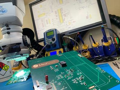
4.3 Inspection and Testing
- Visual Inspection: Checks for soldering defects like bridges or insufficient solder.
- Automated Optical Inspection (AOI): Detects assembly errors.
- X-ray Inspection: Essential for hidden joints in BGA packages.
- Functional Testing: Verifies the PCB operates as intended.
5. Quality Control and Testing
5.1 Electrical Testing
- Continuity Testing: Ensures no open circuits.
- Insulation Resistance Testing: Checks for leakage between traces.
5.2 Environmental Testing
- Thermal Cycling: Assesses performance under temperature variations.
- Vibration and Shock Testing: Validates durability in harsh conditions.
6. Common PCB Manufacturing Defects and Solutions
| Defect | Cause | Solution |
|---|---|---|
| Delamination | Poor bonding between layers | Use high-quality laminates and proper lamination pressure |
| Solder Bridges | Excessive solder or misalignment | Optimize stencil design and reflow profile |
| Open Circuits | Broken traces or poor plating | Improve etching and plating processes |
| EMI Issues | Poor grounding or routing | Implement proper grounding and shielding techniques |
7. Conclusion
Successful PCB manufacturing requires careful attention to design, material selection, fabrication, assembly, and testing. By following best practices in each stage, manufacturers can produce high-quality, reliable PCBs that meet performance and durability requirements. Whether designing a simple single-layer board or a complex multilayer PCB, understanding these key considerations ensures a smooth production process and a functional end product.
By adhering to these guidelines, engineers and manufacturers can minimize defects, reduce costs, and improve the overall quality of PCBs in electronic devices.